
Onto Innovation | The Ultimate Advanced Packaging Comeback
Take share from KLA in backend CoWoS inspection + Take share from Camtek for Micron HBM inspection + WFE Supercycle go brrrr

Opinions are my own and do not represent past, present, and/or future employers. All content is based on public information and independent research. This newsletter is not financial advice, and readers should always do their own research before investing in any security. I am invested in the semiconductor industry. As of the date of this publication, I may hold long or short positions in the securities discussed in this article.
This research is 100% free. I hope you find it helpful, enjoy reading it, or that it makes your day slightly better. If that is the case, I ask that you like, comment, restack, and tell a friend about my work. Sounds cliche, I know, but us creators say this for a reason LMAO. It helps my writing reach and impact more people. I truly appreciate it.
Follow me on X: @jasons_chips. Tryna let more people hear my unhinged tweets.
Onto Innovation inspects packaging.

Outline
Intro to Packaging
Inspection and Metrology Backgrounder
Advanced Packaging Inspection
Fundamental Tradeoffs of Inspection
Algorithms
Infrared
We’re So Back (at TSMC)
The CoWoS-L Transition
Steelman Da Bear
Bull Counter
Dragonfly 5
HBM (High Bandwidth Marketsharegains)
How HBM Inspection is Different
Micron W
Recent Rumor
It’s Modeling Time
Overall WFE Growth
Advanced Packaging Growth
Process Control Intensity
Onto Share Gains
The Model
Intro to Packaging
There was this guy called Gordon Moore who liked to make laws about chips.
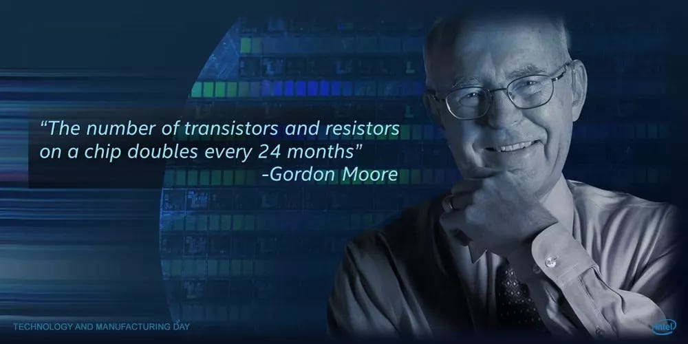
But now, it is slowing down. Today’s transistors are the outlaws and criminals of Moore’s Law. Weird quantum mechanics get in the way when you’re literally dealing with fractions of nanometers. How do we keep making chips faster?
The semiconductor industry’s answer: do not cram more transistors onto one chip. Instead, take multiple specialized chips (called “chiplets”) and connect them together in a single package. One block handles memory, another handles compute, another handles I/O.
This is advanced packaging.
See my backgrounder here. It was originally written as the intro to this article but I decided to publish it separately… and it ended up doing well!

Inspection and Metrology Backgrounder
Inspection & Metrology are an important class of Wafer Manufacturing Equipment (WFE). If you are a player in the market, at the most fundamental level, your tool needs to answer one question for TSMC: “Is this thing built correctly, and if not, where and why did it go wrong?”
The players here are KLA (the 800lb gorilla), Camtek, and Onto. These tools are split into two primary categories: …Inspection and Metrology 😅.
Inspection: Finding defects (binary: is something wrong here?)
Metrology: Measuring dimensions and properties (continuous: how close to spec is this?)
Advanced Packaging Inspection
Advanced packaging is fundamentally about connecting multiple dies together through some combination of:
Metal interconnects (bumps, pillars, pads) that carry electrical signals from one die to another.
Dielectric (insulating material) layers that insulate and planarize (make surface flat).
Through-silicon vias (TSVs) that punch vertically through silicon and connect vertical layers like floors on a building.
Redistribution layers (RDL) that re-route electrical from die pad locations to new ones more suitable for packaging.
Every one of these features can go wrong in ways that kill the package. Your tool needs to catch those failure modes and whisper in TSMC’s ear when you don’t feel so good.

The core failure categories are:
Something is missing or extra — a bump didn’t form, a via didn’t open, a particle landed on a bonding surface
Something is the wrong size or shape — a bump is too short, an RDL line is too narrow, a Cu pad is dished too much
Something is in the wrong place — layers are misaligned, a die is shifted from its target position
Something is wrong internally — a void inside a solder joint, delamination at a bonding interface, a crack propagating through silicon
Inspection is super important as packaging gets more complicated because more layers means exponentially more opportunities for defects.
In a traditional front-end wafer fab, you’re building one chip at a time. A defect kills one die. Annoying, but manageable. You test, you bin, you move on.
In advanced packaging, you’re assembling multiple known good dies (you know the dies are good) into a single package. A defect doesn’t just kill the package — it kills every chip inside it. Uh oh! One bad HBM stack ruins a $30,000 GPU module. One void in a hybrid bond turns a working chiplet into an expensive paperweight.
Advanced packaging inspection falls into three categories:
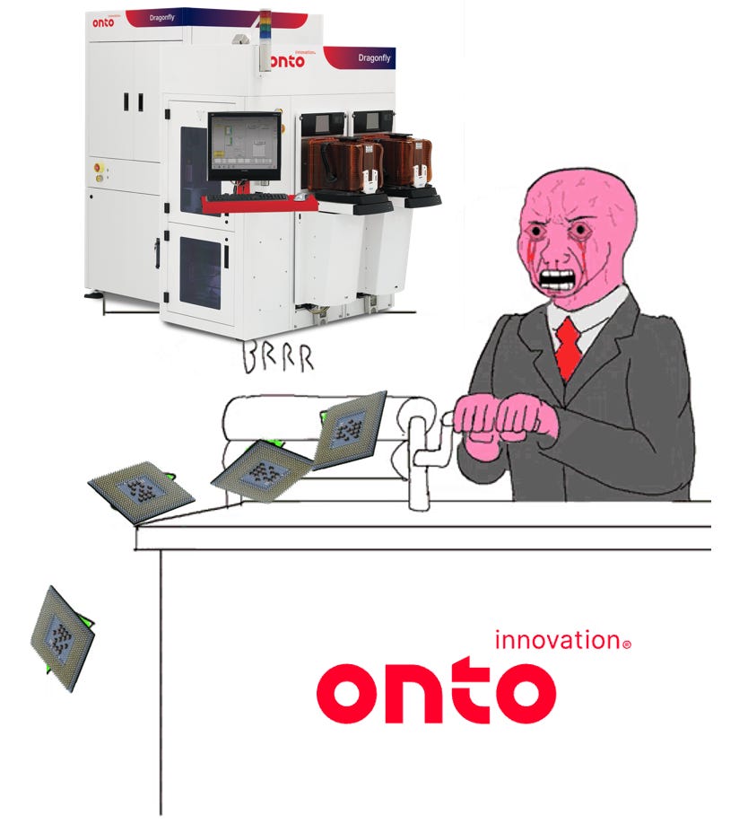
1. 2D Surface Inspection: Looking at the top surface for contamination, scratches, bump damage, missing bumps, and pattern defects. (This is what Onto does with their flagship product, Dragonfly).
2. 3D Metrology: Measuring bump height, coplanarity (are all bumps the same height?), TSV depth, and warpage. Critical for ensuring good contact during bonding.
3. Subsurface Inspection: Finding voids and delamination inside bonded structures. This requires infrared light that can see through silicon. Critical for hybrid bonding and HBM.
Fundamental Tradeoff of Inspection
How do you actually find a 1-micron particle on a 300mm wafer that has billions of features?
Optical inspection works by shining light on the wafer and analyzing what bounces back. A defect (particle, scratch, void) scatters light differently than the surrounding pattern. Your job is to detect that difference.
The challenge is signal-to-noise ratio (SNR). The defect signal is tiny. The background noise (from the pattern itself, from the optics, from the sensor) is enormous. Inspection is fundamentally a pattern recognition problem: distinguishing the “defect signature” from the “everything else signature.”
IT’S REALLY HARD!
Resolution vs. Throughput is the fundamental tradeoff that defines inspection equipment.
Resolution determines the smallest defect you can see. It’s limited by the wavelength of light (diffraction limit) and your optical system’s numerical aperture. Shorter wavelength = better resolution. Higher Numerical Aperture, or NA (yes like that ASML thing) = better resolution.
Throughput determines how many wafers per hour you can process. More pixels per image = slower scanning. Higher magnification = smaller field of view = more images needed.
Makes sense if you think about it. I can do my homework fast or I can do it well.
These two goals are at war. To see smaller defects, you need higher magnification and slower scanning. To process more wafers, you need lower magnification and faster scanning.
Different companies optimize this tradeoff differently. KLA is the spoiled rich kid who prioritizes resolution using their very fancy very expensive machines. They take great pride in their high gross margins (KLA 65% vs ONTO 55%) and won’t ever lower prices even when it costs them market share.
I will communicate what Onto prioritizes via meme.
Algorithms
The raw optical systems are not really that hard to make. Inspection equipment is really a software business.
nonononono not that kinda software
Signal Processing
Funny enough this level of software runs on custom ASICs and GPUs.
Signal processing means you take the raw signal as an input and process the data at the speed the sensor generates it, which is enormous. When you’re scanning a 300mm wafer at high speed with multiple detector channels, you’re generating data at rates of tens of gigabytes per second. You can’t store all of it and process it later so you need to make decisions in real time about what’s interesting and what to throw away.
This layer converts raw sensor output into something the next layer can work with. It’s deeply coupled to the hardware and is essentially firmware.
Defect Detection & Classification (The Core Algorithms)
This is where the intellectual core of the tool lives. It takes the processed signal and answers: is there a defect here, what kind is it, and how bad is it?
Detection fundamentally works by comparison. You need a reference (what the wafer should look like), either by looking at an adjacent die or an example from a database, and then you’re looking for deviations.
Onto uses the die-to-die method. It’s much cheaper and faster and easier, because, well think about it. You just look at the die next to it. That’s a big reason why they have such good throughput. The fundamental tradeoff is unlike die-to-database, die-to-die is blind to systematic defects. Like imagine if every die has the same issue, the machine can’t tell because they still all look the same.
KLA uses the die-to-database method. That means they don’t have the systematic defect weakness, so it’s more robust and they can charge more. However, it’s slower and more expensive. This works for them because they have best-in-class simulation software which is absolutely essential for die-to-database.
After detection, you have thousands of candidate defect events wafer. Most are nuisance (false positives or defects that don’t impact function). Now you need classification to assign each candidate to a defect category (particle, scratch, void, pattern defect, line short, missing bump, etc.) and ideally a severity/kill probability. Sounds like… machine learning! We’ve progressed from
Hand crafted rule-based systems to
Traditional ML — feature extraction fed into classifiers like SVMs or random forest to
Deep learning / CNNs
There’s an inherent cold start problem — when TSMC brings up a new process, there are no labeled defects yet. The tool needs to work reasonably well with minimal training data and improve as production ramps.
If you’ve ever taken a basic college ML class, the following will resonate with you.
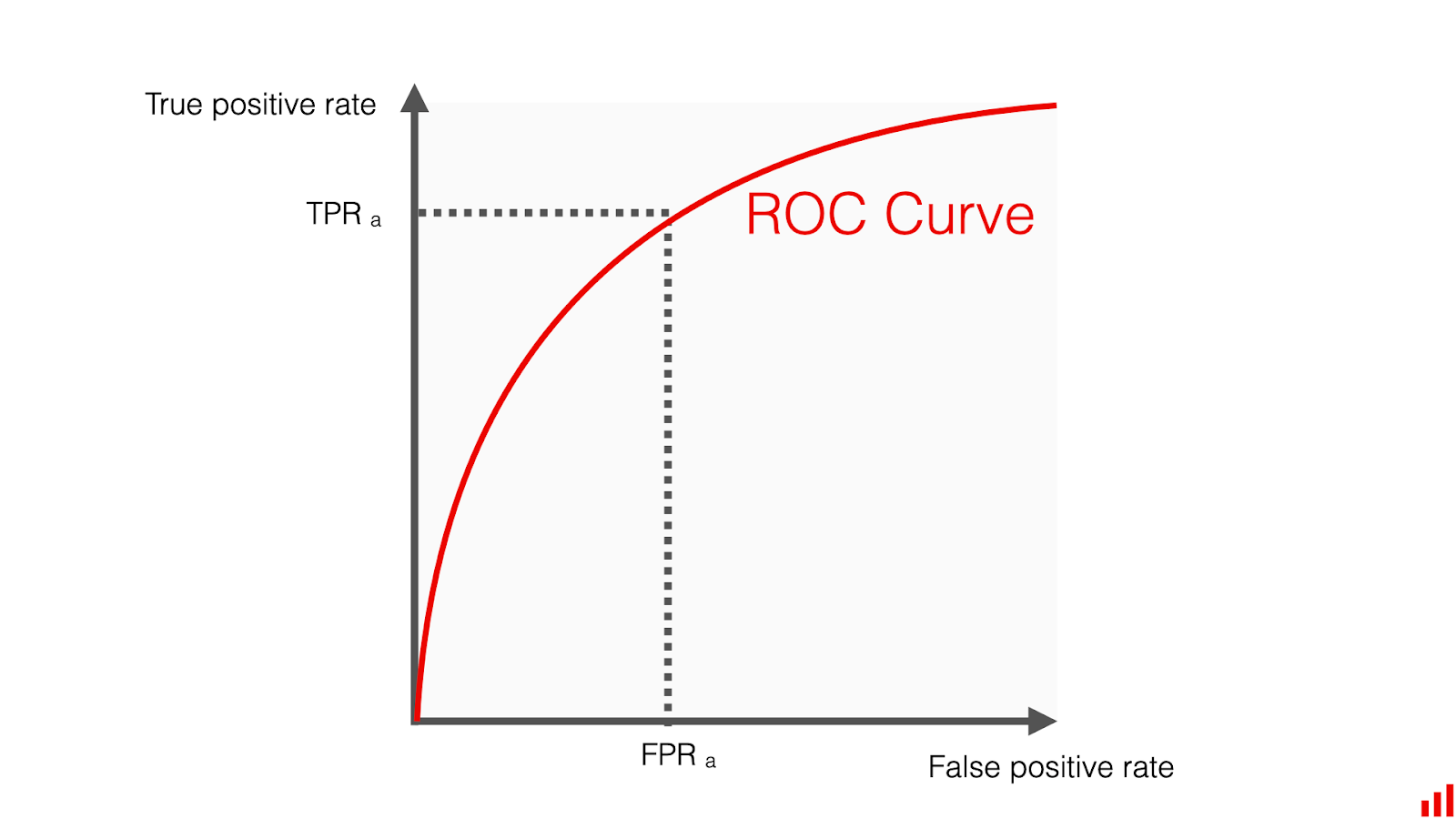
Nuisance filtering involves the sensitivity/specificity tradeoff. If you dial up sensitivity to catch real small defects, your nuisance rate explodes. If you dial it down, you miss killers. The sophistication of your nuisance filter — or your ROC curve (remember that from college?) determines how good your tool is.
Yield Management & Data Analytics
This is the highest and simplest layer. It simply aggregates data across wafers, lots, and time to give process and yield engineers analytics.
Infrared

For HBM and hybrid bonding, you need to inspect inside bonded structures. Visible light can’t penetrate silicon. But infrared can!
Silicon is transparent to wavelengths above ~1.1μm. By using infrared illumination, you can image through the silicon die and see the bond interface below. This lets you detect:
Voids in hybrid bonds (areas where copper didn’t fuse)
Delamination (separation of materials) between stacked dies
TSV defects buried inside the silicon
For HBM inspection, you need to check both the surface (microbumps, contamination) AND the subsurface (voids in previous bond layers). This will also be important later.
We’re So Back (at TSMC)
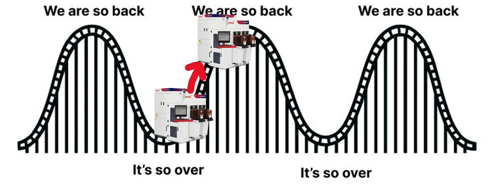
Now let’s talk about what actually happened at TSMC and why it created the opportunity.
The CoWoS-L Transition
TSMC’s CoWoS cake comes in two flavors:
CoWoS-S (”S” for “small” interposer): The OG. Uses a single reticle-sized silicon interposer (~26mm × 33mm). This is what powered every NVIDIA GPU from V100 through H100.
CoWoS-L (”L” for “local silicon interconnect”): The current/next generation. Uses multiple smaller interposer chiplets connected by an RDL (redistribution layer) on an organic substrate. It’s basically EMIB but with the bridges mounted on top of the substrate instead of embedded inside. This allows much larger package sizes, which is why it’s used for Blackwell’s massive GB200 module.
CoWoS-L has different inspection requirements than CoWoS-S.
CoWoS-S used ONTO’s Dragonfly for bump inspection. ONTO had ~70% share of TSMC’s CoWoS inspection at its peak. Life was good.
When TSMC transitioned to CoWoS-L for Blackwell, they needed higher resolution inspection. The previous-generation Dragonfly couldn’t meet the new resolution requirements.
KLA could. KLA’s tools are resolution-optimized. Slower and more expensive, but they hit the spec.
ONTO lost approximately $50 million annualized in CoWoS inspection revenue to KLA during this transition. The stock got hammered.
The bear argument is very straightforward, which I will steelman below.
Steelman Da Bear
Here’s what the bears say to explain the share loss to KLA:
“Aha! You’ve just stumbled upon KLA’s trap card. CoWoS-L is inherently heterogeneous — LSI bridges, organic substrate, and multiple different chiplets create a non-repeating layout with no identical neighbor to compare against, breaking the die-to-die paradigm. Die-to-database solves this by generating a per-location reference from the design file. Hybrid bonding compounds the challenge: tolerances are front-end-like (single-digit nm Cu dishing, sub-0.5nm roughness), and the critical bond interfaces are buried under silicon, requiring either IR through-silicon inspection or extremely reliable pre-bond surface inspection. This obviously means advanced packaging inspection is becoming front end inspection, KLA’s expensive die-to-database tools win, and Onto’s high throughput die-to-die tools lose.”

Bull Counter
I posit that the bear argument is first order thinking, and the second order picture is far different.
Counter 1: TSMC’s switch to KLA was forced and temporary, not structural. Why?
KLA actually doesn’t have a dedicated advanced packaging (backend) product line. This means their tools are tuned to the ultra-clean environment of the front-end and are overly sensitive to the dirtier backend environment. They won the orders despite this drawback because Blackwell was the most important product ramp in semiconductor history and Onto’s tools at the time just didn’t have the resolution needed.
KLA won not because of structural die-to-database superiority, but because of temporary resolution advantage.
Counter 2: TSMC is heavily incentivized to shift share back to Onto. Why?
KLA’s tools are 50% more expensive.
Meanwhile, Onto’s tools provide 2x the throughput due to being dedicated backend inspectors.
TSMC is very careful with supplier diversification. They have too much spend at KLA so Onto presents a compelling way to reduce concentration.
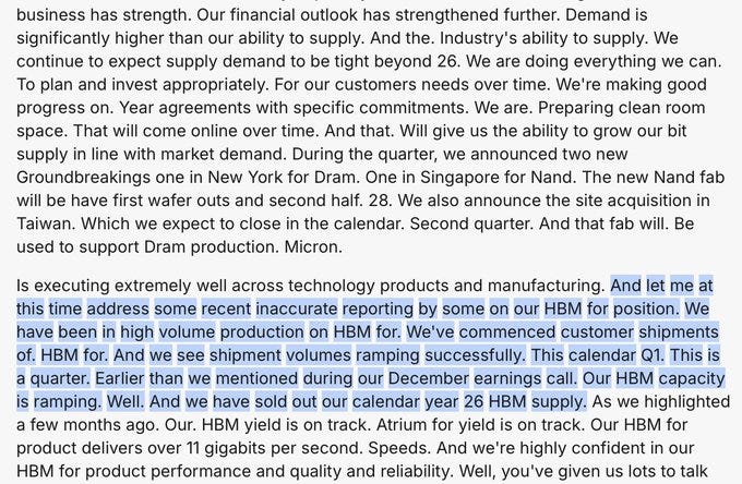
This is not just me saying it. Rick Wallace in KLA’s CY2025 Q3 earnings call regarding TSMC asking for their tools on the backend:
“...that was our initial reaction when the customers wanted us to put our front-end portfolio in the back-end. We said, are you sure? Because the cost of that, are you sure you need it?”
Counter 3: TSMC backend share will stay with Onto even as technology progresses. Why?
The idea that die-to-database is necessary for future backend inspection is greatly exaggerated.

The critical defects across CoWoS-L, HBM4/4E, and hybrid bonding are overwhelmingly random — particles, voids, contamination, alignment errors — not systematic pattern defects. CoWoS-L’s heterogeneity problem is real for die-to-die comparison, but solvable through golden reference comparison and zone-based ML classification rather than full die-to-database simulation. HBM hybrid bonding defects require IR subsurface inspection to see through silicon (Onto’s strength), not design-file comparison. Even pre-bond surface inspection, the closest to front-end-like requirements, is fundamentally about high-sensitivity metrology (measuring dishing, roughness, particles) rather than pattern verification. Die-to-database would only become necessary if packaging RDL patterning (~1-2μm features) starts producing systematic litho defects like front-end processes (~3nm), and we’re orders of magnitude away from that.
Dragonfly 5
Onto developed Dragonfly 5 specifically to meet TSMC’s new resolution requirements while still being a dedicated backend tool.
Dragonfly 5 achieves the required resolution through:
Enhanced optical path with higher NA
New illumination modes optimized for RDL inspection
Algorithm upgrades for finer feature detection
The tool has been shipped to TSMC and they seem far along in the qualification process. They have passed “optical validation” which is NOT qualification but is a very good sign.
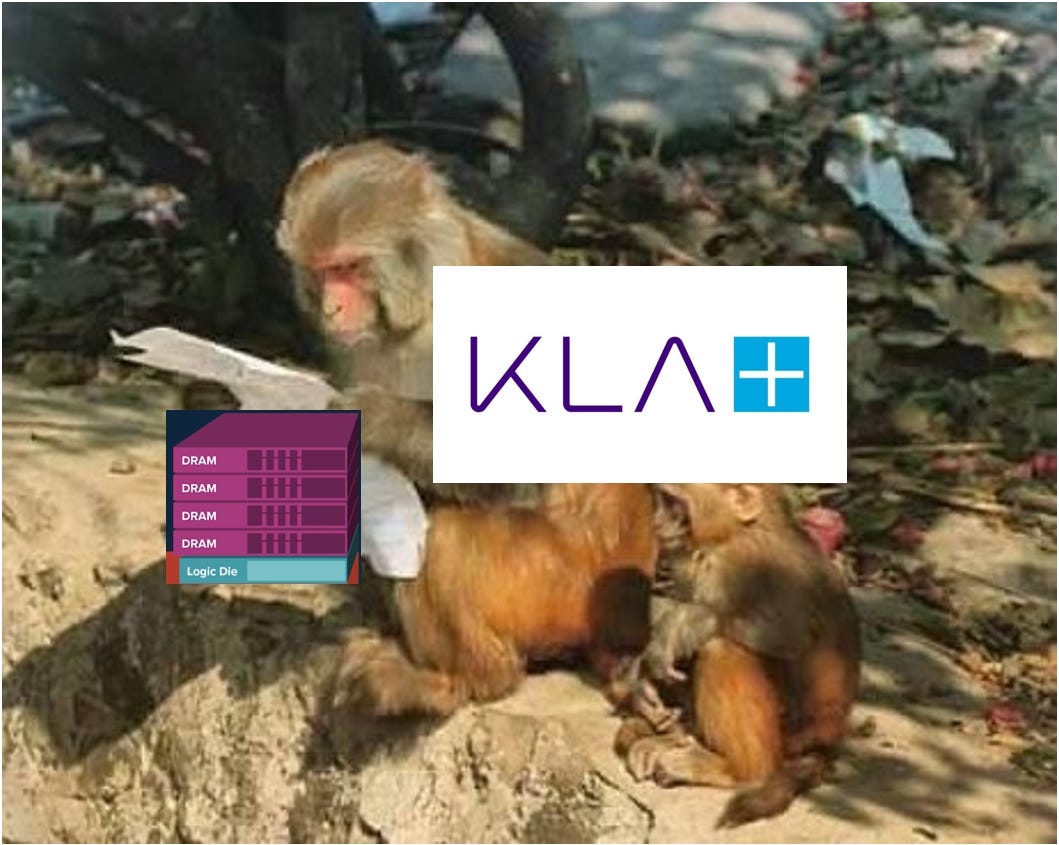
HBM (High Bandwidth Marketsharegains)
In a nutshell, HBM is a bunch of DRAM dies stacked on top of one another. Most of you know this.
How HBM Inspection is Different
First, CoWoS is horizontal — chiplets connected side-by-side on an interposer.
HBM is vertical — stacked DRAM dies.
The inspection goes from left n’ right to up n’ down!
Second, die-to-database inspection is useless for HBM. Every DRAM die is the same design, same process, repeated. The defects that kill HBM yield are all random. Die-to-die comparison catches them perfectly. Die-to-database goes from a tradeoff to having zero benefit.
KLA not only doesn’t have a dedicated HBM inspector, they are completely fucking useless.
When KLA attempted to enter Micron’s HBM inspection, their tools performed worst among all three competitors in side-by-side evaluations. Their front-end-optimized algorithms couldn’t distinguish real defects from noise in the particle-heavy backend environment. Micron rejected them entirely.
Third, there is a need for speed. HBM is a high-volume business, and because the cost of a failed cube (and the CoWoS package it sits on) is enormous, customers are moving toward 100% inspection rather than sampling. When you’re inspecting every die on every wafer, throughput is the single most important competitive axis.
Fourth, HBM inspection splits into two categories.
Wafer-level inspection happens to the wafer before it’s diced n’ sliced. before dicing and stacking. This is the same concept as CoWoS inspection: you’re scanning a 300mm wafer.
Die-level inspection happens to the dies themselves after dicing and during or after stacking. This category does not exist in CoWoS because the CoWoS packaging literally is a wafer. (Chip-on-WAFER-on-Substrate)
Onto has traditionally been strong in wafer-level inspection. Die-level inspection has been dominated by Camtek, particularly at SK Hynix. This starting position is important context for understanding how Onto has been gaining share, which we turn to next.
Micron W
Step 1: The starting position. Micron historically used Camtek for HBM inspection. Camtek had 100% share for wafer-level inspection and dominant share for die-level inspection. Onto had only a small foothold in die-level inspection.
Outside of Micron, SK hynix uses Camtek and Samsung uses Onto.
Step 2: Onto beats Camtek in die-level inspection. Die-level inspection is about inspecting individual HBM cubes after they’ve been diced from the wafer. The defects are relatively large and easy to see optically, so the competitive differentiator is speed. How fast can you scan each cube and classify defects?
Onto optimized the Dragonfly’s alignment algorithms and added GPU acceleration to the image processing pipeline. This achieved a 4x throughput improvement specifically for HBM die-level inspection. Micron switched to Onto as their primary die-level inspection supplier based on this throughput advantage.
Step 3: Onto identifies Camtek’s weakness in wafer-level inspection. Wafer-level inspection is the higher-value, stickier business because it happens earlier in the process and there are more insertion points. Camtek’s dominance here was built on two things: their white-light 3D microbump metrology and their general visible-light 2D inspection.
But Onto’s team identified a gap: Camtek’s visible light tool has no integrated infrared inspection capability. They have a separate infrared tool, but it’s a separate tool.
Micron is pursuing hybrid bonding for HBM4. When you hybrid bond, there are no microbumps, just copper-to-copper fusion. The critical defect type changes completely: instead of looking for malformed bumps on the surface (visible light works fine), you’re looking for voids between bonded copper pads that are buried under silicon (invisible to visible light, requires infrared).
So for HBM4, Micron’s wafer-level inspection needs to include both conventional visible-light inspection AND infrared subsurface inspection. With Camtek, Micron would need to buy two separate tools, one visible-light tool and one infrared tool. Two tools means double the capital cost, double the fab footprint, double the recipe development, and a second wafer handling step that introduces contamination risk.
Step 4: Onto offers an all-in-one solution. The Dragonfly platform has always integrated both visible and infrared on a single tool body, sharing the same stage, wafer handling, and image processing pipeline. This wasn’t built for HBM. Onto inherited infrared expertise from Rudolph Technologies, which had been doing infrared years before hybrid bonding, after the merger. When Onto designed the Dragonfly platform, this multi-modality was the foundational design. For Micron’s HBM4 inspection, this means a single Dragonfly can do conventional visible-light inspection and IR void detection in one pass — one tool, one wafer load, one recipe.
Camtek can’t easily match this without significant risk to their existing business. This is a textbook case of counterpositioning.
Camtek built the best visible-light inspection platform in the industry. Their visible light metrology algorithms are so good that even KLA concedes they can’t compete. But integrating IR requires fundamentally different optics, different sensors, and different illumination engineering. Integrating infrared requires a ground-up redesign — years of engineering effort with significant execution risk.
The very specialization that made Camtek dominant in microbump inspection now prevents them from adapting to hybrid bonding inspection without cannibalizing their own architecture. By the time Camtek could ship an integrated solution, Onto will have years of production-proven IR data and customer recipes at Micron, which is its own moat.
Step 5: Onto passes Micron’s validation. Onto’s all-in-one tool has officially qualified for wafer-level HBM inspection. This is the critical milestone because memory makers are notoriously rigorous about qualification. Once qualified, you’re sticky, and once you’re rejected, you’re out for that generation.
Micron has recently placed HBM inspection orders worth tens of millions of dollars with Onto, for delivery between Q4 2025 and Q1 2026.
Step 6: The flywheel effect. As Onto’s Dragonfly installed base grows at Micron, several reinforcing dynamics kick in. Onto’s algorithms get trained on more Micron-specific defect data, improving classification accuracy over time. Micron’s process engineers build institutional knowledge around Dragonfly recipes, increasing switching costs. And as HBM4 hybrid bonding scales to production, every new line needs the integrated visible + infrared capability that only Onto currently offers on a single platform. Camtek would need to develop an integrated IR solution or accept being relegated to the shrinking microbump-only inspection market.
And final thought I will posit:
If this happened at Micron, why not SK hynix?
Recent Rumor
There has been a recent rumor on Micron’s share of Nvidia HBM falling to 0% because they tried to make the logic base die using their internal DRAM process to save cost instead of outsourcing a logic process to the logic fab TSMC. This is a really stupid idea btw, not only are the cost savings minimal compared to the risk, they also cannibalized DRAM capacity that could have been used for the memory shortage.
However, apparently the rumor isn’t true. Micron stock at all-time-highs.
It’s Modeling Time
I will model Onto using a top-down approach rather than a bottom-up one. Why?
Nobody outside of Onto’s sales team really knows how many Dragonfly units they’ll ship.
However, I will use our growth rates to back out implied shipments and ASPs for illustrative purposes.
Our top-down forecast is informed by 4 factors:
Overall WFE Growth
Advanced Packaging Growth
Process Control Intensity
Onto Share Gains
Overall WFE Growth
2025 total WFE spend was around $115b.
2026, from various discussions and companies and sources I’ve heard, seems to coalesce around $135b.
There is probably upside bias here, and this is probably back-half weighted due to cleanroom constraints.
This lines up with Applied Material’s prediction of 20% WFE growth, which they also believed to have upside bias and to be back-half weighted.
Advanced Packaging Growth
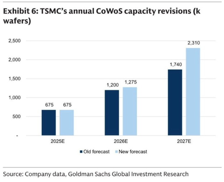
These are Goldman’s CoWoS capacity estimates.
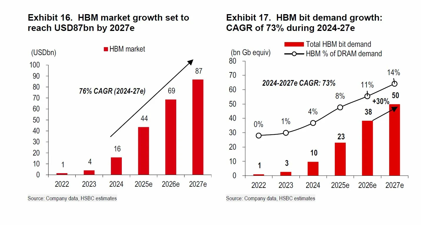
And these are HSBC’s HBM market growth numbers, although I think they are a bit conservative after all those hyperscaler capex hikes. All Nvidia GPUs, of which the hypers are buying a lot of, need HBM.
Another constructive datapoint on advanced packaging capacity growth is Amkor capex: $2.75b vs $1.6b expected. Capex nearly TRIPLED year over year.
Advanced packaging clearly outgrows overall WFE spend, so we can safely say >>20%.
To triangulate it further, lets use TSMC’s packaging revenue and capex commentary:
2025 CapEx: $40.9B, with advanced packaging “about 10%, lower than 10%” = ~$4.1B
2026 CapEx: $54B, with advanced packaging “10% to 20%” = $5.4-10.8B
So 31-163% growth. That sure establishes that it’s high, but not much help.
So let’s see C.C. Wei’s commentary: $52-56B CapEx in 2026 yields “almost none” contribution to capacity this year, and “a little bit” in 2027. Real capacity relief comes 2028-2029.
What does this mean? If capex isn’t translating to capacity relief, that means the capex growth is mostly cleanrooms and facilities and not tools. This squares nicely with very frequent industry commentary talking about cleanroom constraints restraining WFE growth until H2 2026. Therefore, 2027 growth should be faster than 2026 as TSMC’s capex on cleanrooms serves as a leading indicator for tool demand.
For sake of simplicity, let’s assume advanced packaging tool growth of 25% in 2026 and 35% in 2027.
Process Control Intensity
Process control, including inspection, is the fastest growing class of tools within advanced packaging as complexity increases its criticality.
Let’s listen to KLA to triangulate this:
2021: KLA was 10% of total AP process control market, and AP process control was 1% of total AP equipment
2025: KLA is “close to half” of AP process control market, and AP process control is 6% of total AP equipment
So AP process control as a share of total AP equipment went from 1% to 6% in four years.
Now, that ain’t sustainable. It was driven by the initial adoption phase where packaging went from barely needing inspection to requiring serious process control almost overnight. The intensity uplift should moderate as the base gets bigger and the most critical inspection insertion points are already established.
Where does it settle?
KLA gave us another anchor. Bren said on Q3 that KLA’s share of overall WFE (including front-end) is ~8%, while their share of AP specifically is ~6%. He said AP process control intensity is “still below” the front-end. Front-end process control intensity is roughly 12-14% of front-end WFE. AP is at 6% and rising toward that level but not there yet.
So the ceiling is roughly 12-14% (front-end parity), current level is ~6%, and we’re somewhere on the curve between them. The rate of convergence toward front-end levels is the intensity uplift.
Let’s assume a 1.3x multiplier for inspection growth vs total advanced packaging growth to account for this. So 32.5% inspection growth in 2026 and 45.5% inspection growth in 2027.
Onto Share Gains
The entire point of the first 80% of the writeup was to argue Onto would gain share from its competitors and outgrow the market. I’ll assume most of this happens in 2026 as Dragonfly 5 is already shipped to TSMC and could be qualified soon, and IS qualified at Micron.
For TSMC CoWoS share reversion, Onto lost $50M annualized revenue to KLA. Let’s assume $25M recovered in 2026, $40M in 2027.
For Micron HBM displacement, I have heard that orders placed for Q4 2025-Q1 2026 delivery are in the range of “tens of millions.” Let’s say a conservative estimate for this is $30M in 2026, $50M in 2027 as HBM4 scales.
I estimate 2025 Dragonfly revenue to be $484M. If the AP inspection market grows 32.5% in 2026, Onto growing at market rate alone would give ~$641M. The share gains above add 11.5% to growth in 2026 and 8.5% in 2027. Adding that to our overall inspection growth of 32.5% and 45.5%, we get 44% and 54% growth for Onto Dragonfly in 2026 and 2027 respectively.
Add in some gross margin expansion and our model is complete!
The Model
This research was 100% free. I hope you found it helpful, enjoyed reading it, or that it made your day slightly better. If that was the case, I ask that you like, comment, restack, and tell a friend about my work. Sounds cliche, I know, but us creators say this for a reason LMAO. It helps my writing reach and impact more people. I truly appreciate it.
Thorough and helpful as usual! Great analysis and explanation, I love learning from your posts. 🎉
always enjoy reading your stuff Jason. Whats your thoughts on the recent CAMT earnings?