
The Aixtron Series | Part 2: The Optoelectronics Supercycle
What everyone is missing about Aixtron’s optical networking business + full Revenue Build

Opinions are my own and do not represent past, present, and/or future employers. All content is based on public information and independent research. This newsletter is not financial advice, and readers should always do their own research before investing in any security. I am invested in the semiconductor industry. As of the date of this publication, I may hold long positions in the securities discussed in this article.
Hope everyone enjoyed their Christmas!!! Thank you to anyone who subscribed or pledged. It means the world to me that you found my research helpful and wanted to support.
Because of a series of unfortunate happenings, my next Lumentum writeup is delayed until mid-January. But the model is done, so don’t worry, parts 2-4 will come out in quick succession after that.
However, in the meantime, I have discovered even more about Aixtron that I wanted to share so I am going to be publishing parts 2 & 3 for Aixtron first.
Aixtron has been gaining a lot of attention recently. Multiple (very cool) authors on substack including Irrational Analysis, Fabricated Knowledge, and The Swiss Transparent Portfolio have posted pieces on it. Go check out their work and support them. Kerrisdale Capital initiated a position and posted their in depth research on their website. Even the sell side has gotten more involved—JPMorgan released their initiation (at neutral…) and BofA double upgraded from underperform to buy (lmao).
(To my buysiders, how often do you see a double upgrade by the street?)


Semicap Stock Idea - by Doug O’Laughlin
https://kerr.co/aixa
I have a view on this company that is slightly different from each of those analysts above, particularly on the optoelectronics segment. As was the case with Lumentum, Aixtron has many different business segments, and each investor that is long this stock focuses on a different segment, thus has a totally unrelated thesis as to why it’s mispriced. I love these kinds of companies because of the margin of safety they provide. Be right on just one of them and you have a multibagger upside.
Be right on all of them… and well… take a peek at the Lumentum chart.
Before we get started, please read part 1 of The Aixtron Series for the background necessary to understand today’s writeup.
The Aixtron Series | Part 1: Power Electronics

Hello and welcome to my Substack! Updating this about 45 days since it was published as there are many new readers to whom I want to introduce my writing and publishing style.
The Counter to the SiC Bear Case
My previous writeup highlighted SiC as the key bear case sell-side points to for why Aixtron will miss estimates in the near to medium term. To sum it up, from 2020-2023, there was a massive overinvestment in SiC epitaxy because everyone expected the EV boom to be sunshine and rainbows forever. Fast forward to now, and SiC fabs are so glutted they are operating at 20-30% utilization (capital cycle go brrr). Who would buy a $4mm epitaxy machine for years in this market? In addition, China is rapidly accelerating their semiconductor self-sufficiency, which should give customers every reason to buy domestically vs from Aixtron.
This bear case was what I argued created the conditions for the low share price and attractive entry. However, even this bear case has two major caveats which can lead to a SiC rebound, believe it or not.
The first caveat is that “Chinese Competition” is not quite what it seems. While it is true that domestic Chinese toolmakers like Naura and AMEC are making strides, they are primarily building Single-Wafer tools. These tools process one wafer at a time—great for R&D or small batches, but terrible for cost-efficiency. Aixtron, on the other hand, dominates because of its G10-SiC Batch Tool, which uses the proprietary planetary rotation design to process multiple wafers simultaneously. In a commodity market like SiC, where the only thing that matters is “Cost Per Wafer,” a batch tool that can churn out 9 or 18 wafers at once simply crushes a single-wafer tool on economics. China can build all the tools they want, but if using them costs 30% more per chip, commercially viable fabs will still knock on Aixtron’s door.
The second caveat is the irresistible gravity of the 200mm (8-inch) transition. Right now, the global glut is in 150mm (6-inch) capacity. But the industry is aggressively moving to 200mm wafers because the math is undeniable: a 200mm wafer yields roughly 80% more die per wafer than a 150mm wafer, driving the cost per device down by over 50%. This creates a “forced upgrade” cycle. Even if a fab has empty 150mm lines collecting dust, they cannot afford not to buy new 200mm tools, because staying on the smaller size means structurally higher costs than competitors. This is why Wolfspeed, Infineon, and STMicro are still buying Aixtron’s G10 tools despite the downturn. They aren’t expanding capacity; they are swapping their old, expensive engines for new, efficient ones to survive the price war.
Also, the 200mm transition is a market share donation machine. As Kerrisdale Capital points out, growing a perfect crystal on a small 150mm wafer is hard; growing it on a massive 200mm wafer without warping or cracking is exponentially harder.
SiC is the most fragmented market, with Aixtron still holding the leading share but only 35%, compared to other markets where they have a practical monopoly. As smaller players fail to keep up, consolidation directly benefits Aixtron who can potentially increase their share to 40-50%.
Power Electronics Modeling
Since I skipped the model in my last Aixtron piece, I want to include the GaN and SiC projections here, as well as include some updates on how my thoughts around the SiC business have changed.
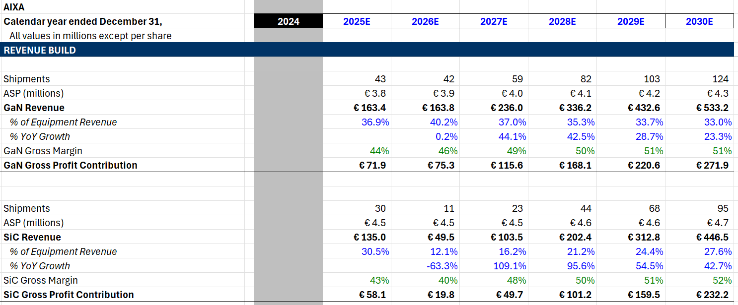
For GaN, we forecast a tangible acceleration in tool shipments starting in 2027. This timeline aligns with the architectural shift in data centers to 800V DC racks, which necessitates the adoption of GaN-based Intermediate Bus Converters (IBCs) for efficient voltage stepping, as we discussed in the previous part. We model ASPs rising steadily throughout the decade. The shift from “Consumer GaN” (chargers) to “Datacenter GaN” requires a move from smaller, simpler platforms to the larger 200mm G10-GaN platform. The G10 commands a premium price due to its ability to handle thick epitaxial layers on silicon substrates without bowing. Finally, we project gradual margin expansion in this segment. As the sales mix shifts toward these high-performance data center tools, the unit economics improve compared to the commoditized consumer tools.
For the SiC segment, our model reflects a “U-shaped” recovery that acknowledges the current overcapacity while preparing for the inevitable upgrade cycle. We model massive digestion in the near term, in line with the most bearish street estimates. We have significantly cut SiC revenue expectations, modeling it to drop below 15% of total equipment revenue during this period. We also model flat ASPs as utilization rates at 150mm fabs remain low (20–30%). However, in 2028+, we model a sharp resurgence. This is not driven by capacity expansion, but by the 200mm transition. As fabs retire 150mm lines to capture the ~50% die cost reduction offered by 200mm wafers, they must purchase new compatible equipment. We also explicitly model Aixtron’s market share growing from 35% today to 40–50% by 2030. This is based on the physics of the G10-SiC batch tool, which offers superior economics on 200mm wafers compared to single-wafer competitors. Consequently, we model SiC gross margins troughing at 40% during the 2026 price wars, before recovering to 52% by the end of the decade as the premium G10 platform becomes the industry standard.
Optoelectronics
This is where I have a serious variant view from both the buyside and the sellside.
To recap, optoelectronics is the end market for anything optics networking related. By happenstance a lot of the stuff that goes in transceivers requires epitaxy.
Monopoly!
In SiC, Aixtron needs to fight for every order.
In Optoelectronics, Aixtron decided to pull an ASML and basically corner the whole market. They have over 90% share!! (!!!)
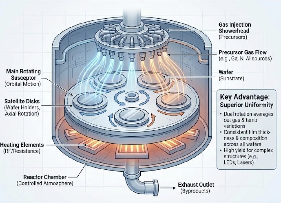
The dominance again comes down to the unique capabilities of its “Planetary Reactor” design.
In SiC (vertical furnaces) and GaN (single-wafer tools), the competition is fierce because the “recipe” for growing these layers is well-understood and can be replicated by competitors like AMEC or Veeco using similar showerhead designs.
However, Optoelectronics (Lasers and MicroLEDs) requires a level of precision that standard tools simply cannot match. Aixtron’s proprietary Planetary Reactor technology uses a “dual-rotation” mechanism where the wafers orbit the center of the chamber while simultaneously spinning on their own axis. This creates a specific gas flow dynamic that achieves near-perfect uniformity across hundreds of layers of Indium Phosphide (InP) or Gallium Arsenide (GaAs).
For a laser, layer thickness uniformity determines the wavelength of the light. If your thickness varies by even a few atomic percentages, the laser’s color (wavelength) shifts, and the device is useless for high-speed data transmission. Competitors’ tools, which often use simple single-rotation susceptors, struggle to maintain this uniformity at the edges of the wafer, leading to massive yield loss. Because the physics of the Planetary Reactor are patented and incredibly difficult to engineer, customers like Lumentum and Tower simply cannot switch to a competitor without crashing their yields.
In conclusion, if you want to manufacture the lasers that connect Nvidia GPUs, you effectively have two choices:
Buy an Aixtron tool.
See choice #1
Lumentum and Tower Semi
Shamelessly plugging my Lumentum pt 1 writeup here:

Also might do a series on Tower at some point.
To understand why tool demand is about to explode, you need to understand who is actually buying from Aixtron: Lumentum and Tower Semiconductor. Coherent and others are also customers, but I believe Lumentum and Tower will see the strongest capex inflections soon.
Lumentum is the leading Indium Phosphide (InP) laser manufacturer. These are the light sources for any optical transceiver.
Tower Semi is the leading silicon photonics (SiPho) fab. They manufacture silicon chips that guide and modulate light and have their own Process Design Kit (PDK) fabless designers use, just like TSMC. GlobalFoundries and TSMC compete in SiPho too but Tower has a commanding lead.
These two companies do very different things but share one commonality: They both need boatloads of Aixtron’s epitaxy stuff. Lumentum needs it for the InP fabrication, while Tower needs it to grow SiGe layers for the active components on SiPho chips (drivers, TIAs, photodiodes).
Both of these companies have recently signaled that demand is off the walls.
On Lumentum’s recent Q1 FY26 earnings call, CEO Michael Hurlston was blunt about the state of the market:
“Demand is increasing so strongly that the company is fully allocated and is falling further behind demand even as it significantly increases capacity... We’ve added manufacturing capacity in Thailand to support that... but our general view is, it’s limited for now.”
They are upping capacity by 40% over the next few quarters, but are still running behind demand and are SHEDDING customers. Think about how insane that is.
Now, Tower is seeing just as dramatic of an inflection. On their Q3 2025 call, CEO Russell Ellwanger described the ramp for their SiPho platform:
“We are seeing unprecedented demand for our Silicon Photonics platform... driving what we believe will be unprecedented company growth... “
“Silicon photonics continues to increase market share over EML solutions, given its significant cost advantage. SiPh typically requires half the number of lasers as an equivalent EML product, with performance benefits especially seen at 1.6T. As such, we anticipate this market share shift to be permanent.
Hence, we are at this point going to add additional CapEx to address an even increased surging demand.”
The point is, both companies are scrambling to add capacity. “Adding capacity” makes Aixtron very happy because they get to sell a shit ton of their stuff and make lots of money.
Why Tower Must Add Capacity
Now we shall cover the actual science behind why these customers are seeing such massive inflection points, starting with Tower and their SiPho.
For the last decade, the optical industry has relied on Indium Phosphide (InP) transceivers. These are high-performance but incredibly difficult to manufacture. They are typically grown on small, fragile 3-inch or 4-inch wafers.
But as we move from 800G to 1.6 Terabits (1.6T), SiPho wins because of the brutal economics of Yield. Remember the Tower CEO saying how SiPho had a massive cost advantage?
Traditional InP manufacturing is a nightmare of “boutique” fabrication. The wafers are small, brittle, and prone to breakage. When you process a 3-inch InP wafer, you might get a few hundred good dies. The edge yield is terrible, and the “touch labor” is high.
Tower Semiconductor is changing the game by manufacturing optics on 300mm (12-inch) Silicon wafers. A 12-inch wafer has 16x the surface area of a 3-inch wafer, so instead of getting 500 chips per run, Tower gets 8,000+ chips per run. Because they use standard CMOS tools (the same ones used to make logic chips), the defect rates are infinitesimal compared to a boutique laser fab.
Tower CEO Russell Ellwanger wasn’t subtle about this on the Q3 call. He explicitly linked the “unprecedented demand” to customers needing to solve capacity bottlenecks. Meaning the industry cannot produce 1.6T optics at Nvidia-scale using the old InP methods. They must move to the SiPho foundry model. And this transition forces Tower into adding capacity that would otherwise be absorbed by existing InP plants from Coherent.
Why Tower’s Equipment Mix Will Shift Towards Epitaxy
Beyond increasing overall capex, Tower must shift their equipment mix toward epitaxy.
The first driver here is the industry’s move toward Linear Pluggable Optics (LPO). In a standard transceiver, a power-hungry Digital Signal Processor (DSP) cleans up the signal. LPO removes this DSP to save massive amounts of power and reduce latency. But there is no free lunch: when you remove the digital DSP, the analog components (the Driver and TIA chips) have to work much harder. They must take on complex tasks like “continuous time linear equalization,” which significantly increases the physical size of the silicon germanium die required for every unit. Since SiGe layers are created exclusively through epitaxy, the shift to LPO means Tower has to order more epitaxy equipment.
The second driver is the need to integrate InP modulators directly onto the silicon for next gen data rates past 3.2T. This is the holy grail of photonics: combining the scale of silicon with the speed of InP. This process requires heterogeneous integration; growing and bonding these materials together with atomic precision, which again requires incremental epitaxy equipment.
Why Lumentum Must Add Capacity: Scale-Up Optical Networking and CPO
Scale out is what most people associate optics with today. Ethernet or Infiniband that connects one server rack to another. This is where 800G and 1.6T transceivers live. It’s growing pretty damn fast and is enough of an investment thesis for many optical-exposed companies today.
Scale up instead connects GPUs to each other inside the cluster so they can act as one giant brain. Nvidia’s scale up technology is called NVLink and is a major reason why their moat is so strong. Scale up requires extremely high bandwidth and is historically done with copper.
However, as we approach the physical limits of physics, copper is hitting a wall. At the blistering speeds of 1.6T and beyond per lane, copper cables become too thick, too heavy, and lose too much signal over even short distances. To maintain the bandwidth required for next-generation clusters, the connection must switch from electricity to light. But you cannot simply jam thousands of standard pluggable transceivers around a GPU; they are too bulky and power-hungry to support that level of density. The industry’s solution is Co-Packaged Optics (CPO): moving the optical engine off the faceplate and placing it directly onto the chip package, millimeters from the GPU. While CPO is currently a necessity for these massive Scale Up architectures, it is worth noting that as bandwidth demands continue to double, this density advantage will eventually force Scale Out Ethernet systems to adopt CPO as well, likely at the 3.2T or 6.4T generation.
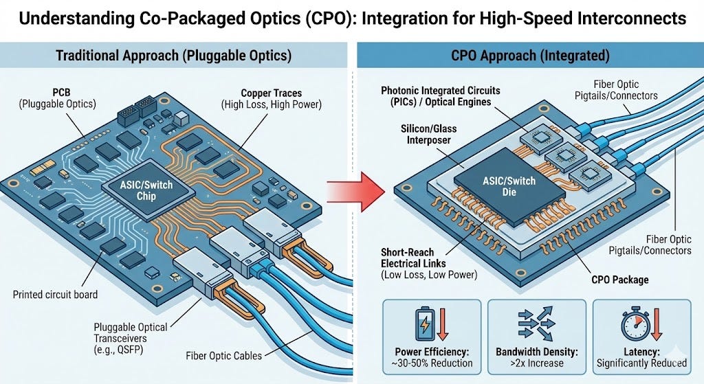
The move to CPO introduces a new thermodynamic problem: heat. GPUs run incredibly hot, and lasers are notoriously sensitive to temperature. If you place a laser directly next to a GPU running at full tilt, it will degrade and fail rapidly. To solve this, the architecture splits the transceiver in two. The signal processing components (modulators) stay on the hot GPU package, but the actual light source is moved to a separate, cool box elsewhere in the rack. This box is called the External Laser Source (ELS).
This architectural split creates a distinct new market for Lumentum. An ELS doesn’t use the small, blinking lasers found in standard transceivers. It requires Ultra High Power (UHP) CW Lasers—massive “light cannons” that generate a continuous, powerful stream of light to be distributed across multiple GPUs. These lasers are significantly larger, more complex to manufacture, and require far more epitaxial precision than commodity components. As Nvidia and others ramp these optical Scale Up architectures, they aren’t just buying more lasers; they are buying a fundamentally different class of laser, one that Lumentum is uniquely positioned to supply and that requires significantly more capacity to produce.
And it is these UHP lasers that are an epitaxy goldmine!
First, to handle that much power without melting, the laser die must be physically larger—often 2x to 3x the size of a standard laser die. Larger dies mean fewer chips per wafer.
Second, in semiconductor manufacturing, yield is a function of surface area. The larger the chip, the higher the probability that a speck of dust or a crystal defect lands on it and kills it. UHP lasers have inherently lower yields than commodity lasers.
Third, to achieve high power efficiency, the epitaxial layer structure (the “Atomic Tetris”) must be much thicker and more complex to prevent electron leakage. This means the wafer has to sit inside the Aixtron reactor for significantly longer.
If a standard laser takes 4 hours to grow and you get 5,000 per wafer, that’s one tool demand profile. If a UHP laser takes 6 hours to grow (complexity), is 3x larger (fewer per wafer), and has 50% lower yield...
You don’t just need a few more tools. You need 5x to 10x the number of Aixtron reactors to produce the same number of lasers.
Optoelectronics Modeling
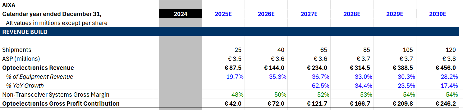
We model a steady acceleration in shipments through the end of the decade. Our 2027 shipment forecast surpasses the most bullish sell-side expectations by approximately 30%. This delta reflects our view on the incoming capex acceleration by Aixtron’s biggest customers combined with the increase in epitaxial intensity of each capex dollar.
We model steady ASP increases throughout the forecast period. Due to Aixtron’s monopoly and optical networking becoming the hard bottleneck for AI scaling, customers like Lumentum and Tower are not price-sensitive on these tools. They will pay a premium for the G10-AsP platform because it is the only tool that guarantees the uniformity needed for UHP lasers. Accordingly, we model Gross Margins expanding to the mid-to-high 50s.
LED
Last (and probably least) is Aixtron’s LED segment. All LEDs require epitaxy because transforming electricity into light demands a flawless, atom-by-atom crystal structure where layers align perfectly to allow electrons to recombine efficiently, a level of precision that standard deposition cannot achieve. This is Aixtron’s smallest business segment but includes a surprising call option.
What is a Regular LED? Think of the screen you are looking at right now. It works like a stained-glass window. At the back of the screen, there is a panel of “Regular LEDs” that act as a backlight. That white light shines through a layer of liquid crystals (the stained glass) which blocks or filters the light to create colors. These LEDs are cheap, easy to make, and we have mastered the manufacturing for decades.
What is a MicroLED? In a MicroLED display, each individual pixel is its own tiny LED. These aren’t the size of lightbulbs; they are microscopic, smaller than a grain of pollen. A 4K MicroLED screen doesn’t have a backlight; it is a mosaic of 24 million distinct, microscopic crystals (Red, Green, and Blue) that turn on and off independently. Now if you heard of OLEDs, this probably sounds similar. However, unlike OLEDs (which use organic, plastic-like materials that degrade and burn in), MicroLEDs are inorganic. They are semiconductor crystals. This means they are blindingly bright, incredibly power-efficient, and they effectively last forever.
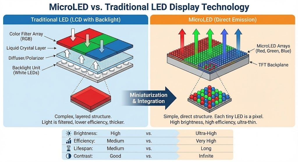
The “Killer App” for MicroLED is Augmented Reality (AR) and wearables. If you are building smart glasses (like the eventual “Apple Glasses”), you have a physics problem: you need a display that is transparent, yet bright enough to compete with the actual sun when you walk outside. OLED cannot get bright enough without melting the battery or burning out the screen. MicroLED is the only technology capable of delivering “daylight brightness” in a microscopic footprint with all-day battery life.
MicroLEDs require significantly more epitaxy because swapping a single large backlight chip for millions of microscopic, distinct crystals causes the total surface area of epitaxial growth required per screen to be exponentially higher. Furthermore, because these pixels are microscopic, the epitaxial uniformity must be nearly perfect across the entire wafer to prevent “wavelength drift” (color mismatches), demanding far more precise and intensive reactor cycles than standard commodity LEDs.
This is why the TAM (Total Addressable Market) here is so explosive. A single smartphone display requires millions of MicroLEDs, so if even a fraction of the high-end wearables or AR market shifts to MicroLED, the demand for epitaxy tools goes parabolic.
LED Modeling
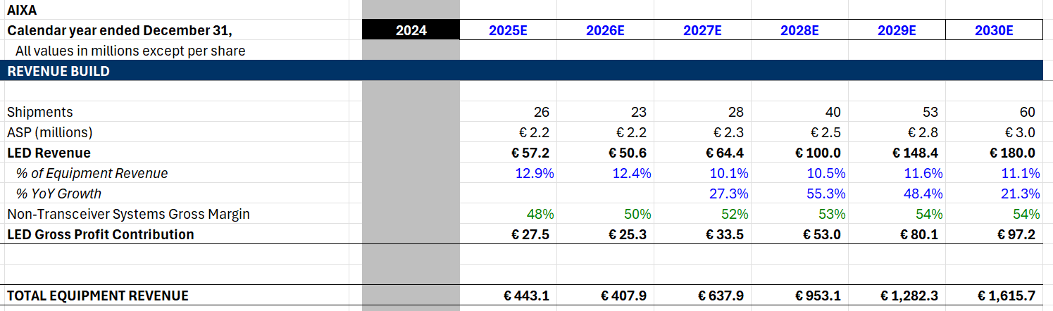
For the LED segment, our model assumes a “K-shaped” divergence. We are effectively writing off the legacy business to focus entirely on the high-value transition to MicroLED.
We model shipments remaining relatively flat in the near term (2025–2026) as the traditional Red-Orange-Yellow (ROY) LED market remains commoditized and saturated. However, we forecast a significant ramp starting in 2027. This is driven by the transition of MicroLED from “R&D Pilot Lines” to “High-Volume Manufacturing” for smartwatches and next-gen automotive displays. We are not modeling a speculative 100-million-unit iPhone adoption; we are modeling a focused ramp for high-end wearables, which alone requires substantial reactor capacity.
More importantly, we project a massive acceleration in blended ASPs. Currently, the LED mix includes lower-cost legacy tools used for standard signage and lighting. As the mix shifts toward MicroLED, the “Average” price skyrockets. A MicroLED reactor (G10-AsP) is a high-precision instrument that commands a multiple of the price of a standard LED tool.
Consequently, we model margins expanding from the low-40s to the corporate average (~50%) by 2028. We are effectively shedding the lowest-margin revenue (commodity LED) and replacing it with some of the highest-margin revenue (MicroLED), creating a structural tailwind for profitability that is completely independent of volume growth.
Conclusion
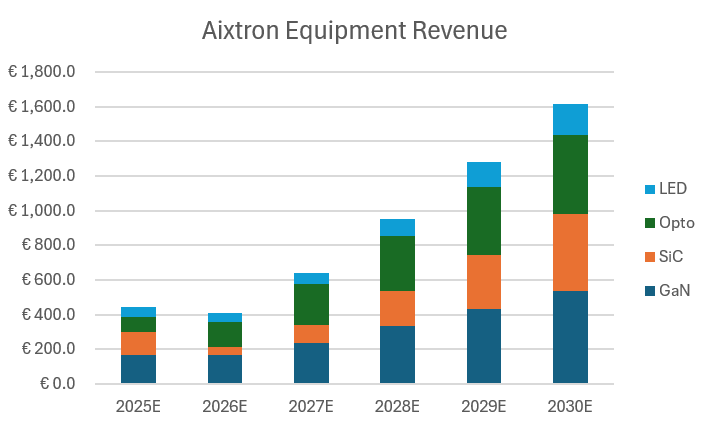
Our model shows total equipment revenue reaching 1.6 billion euros by 2030. The contribution from GaN, Optoelectronics, and SiC are similar after SiC recovers from its trough.
Up Next
What I’ve learned in brutal fashion from the markets is to always be careful of napkin math. Revenue figures could look amazing until the entire DCF present value gets trashed by capex, dilution, etc.
The mantra—build out the model or get screwed when you HODL.
The financials reveal so much about the business quality. And this quality is the main source of the magic with Aixtron. Many small financial nuances that aren’t caught by the markets add up to really drive the upside home.
I will cover this in part 3. Subscribe so you don’t miss it!!
Very interesting, thanks Jason. Out of interest, have you looked at Suss Microtec? Another near-monopoly overlooked EU stock in critical segments of the supply chain which I believe to be criminally undervalued.
Thank you Jason, it was very helpful!