
Short n' Casual Intro to Packaging
Amusing and understandable semiconductor packaging for generalist investors


If I gave you a die, fresh from the fab in Taiwan, it is worse than useless. It will get contaminated and damaged and cannot connect to the PCB.
Semiconductor packaging serves 3 distinct purposes.
Protection: From physical damage and chemical contamination.
Connection: To the rest of the stuff on the PCB.
Translation: Of signals from the microscopic world of the die to the macroscopic world of the board.
The north star of the industry is quite simple. Maximize interconnect density, or how many connections from the chip to the outside world can you fit per square millimeter. An alternative way to say the same thing is pitch, or how far those interconnects are spaced apart. The denser your interconnects, the faster stuff and things move between the chips and the better your GPU functions.
Outline
Wirebonding (1960s-1990s)
Flip-Chip (1990s-2010s)
2.5D Interposers (2010s-present)
3D Stacking and Hybrid Bonding (now-future)
The Interconnects Are Really Dense
Wirebonding (1960s-1990s)
The quintessential OG. Tiny gold wires connect the chip to the package like miniature suspension bridges. Simple and cheap, but the wires create electrical bottlenecks. Still used today for low-performance chips.
There is a very easy way to remember what wirebonding looks like:
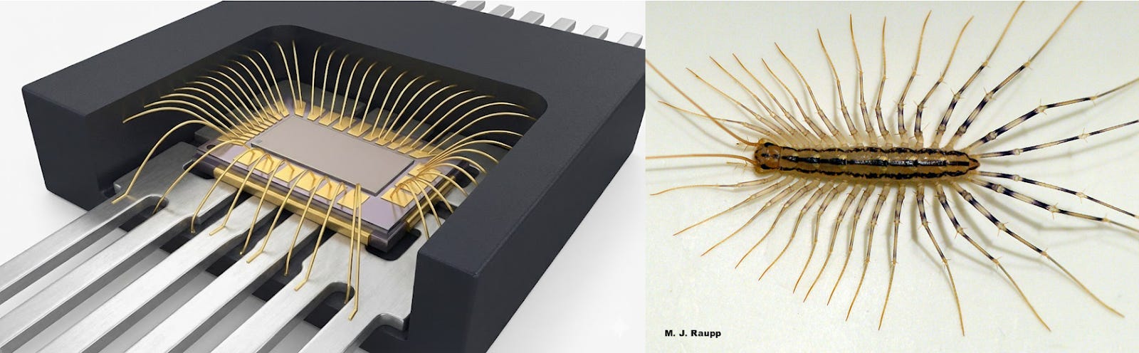
The problems are obvious: It takes up a ton of space! You cannot pack connections together very tightly.
Flip-Chip (1990s-2010s)
Flipping chips was one of the most transformative inventions in the semiconductor industry. Some smart guy once asked:
“Why are we only using the edges of the chip? That is not very much surface area for connections.”
Instead of wires on top, flip the chip face down and connect it directly to the package through tiny solder bumps on the face. More connections, shorter paths, better performance. This is still the workhorse for most processors.
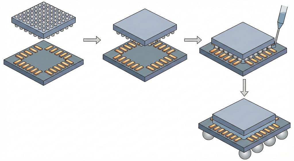
The main problem in flip chip is a mismatch in the Coefficient of Thermal Expansion (CTE). Different things expand differently under high temperatures. So they use underfill where a mold is inserted between the chip and the substrate. This is also the basis of the technology behind SK hynix’s renowned MR-MUF HBM packaging.
2.5D Interposers (2010s-present)
One day, another engineer had a thought.
“Why is building another whole box for chips necessary for achieving protection, connection, and translation?”
It wasn’t. Enter Wafer Level Packaging (WLP). Now, you can build the packaging directly on the wafer itself using the same lithography and etching tools used for fabbing, making life much easier.
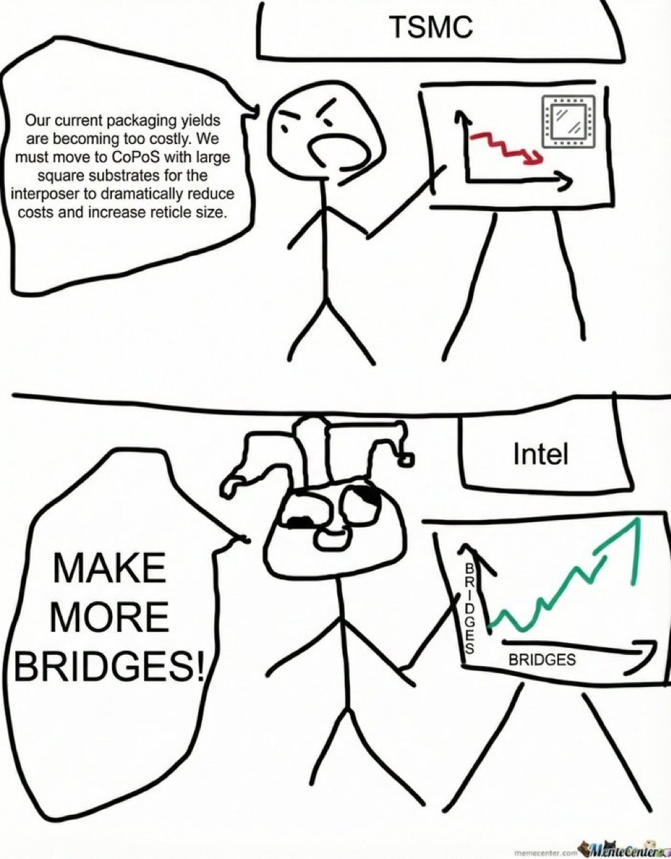
This philosophy led to perhaps the most famous packaging technology today: CoWoS!
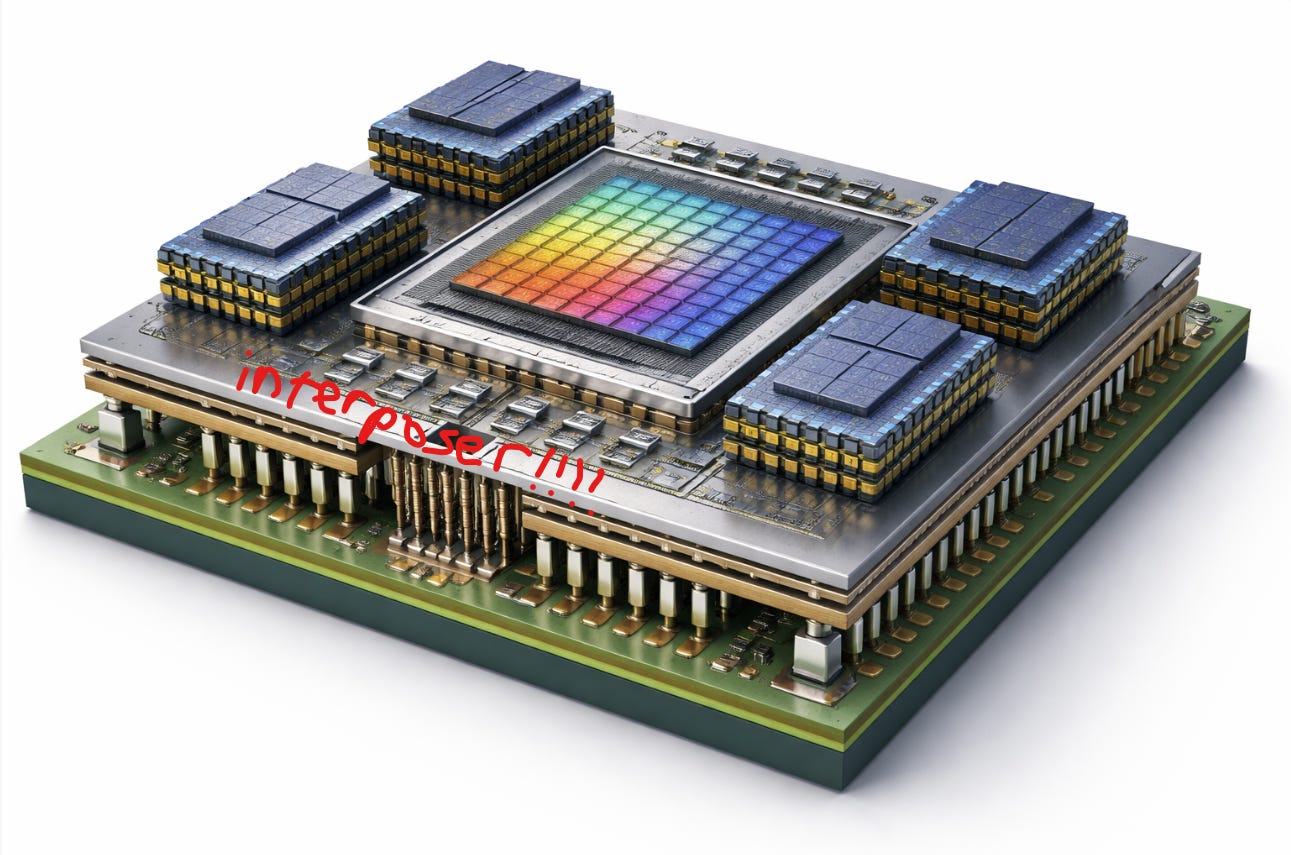
Place multiple chips side-by-side on a silicon “interposer,” a piece of silicon that sits under the chips but ISN’T a chip itself, essentially a passive routing layer that connects them with incredibly dense wiring. This is how NVIDIA connects its GPU die to HBM memory stacks in every AI accelerator you’ve heard of.
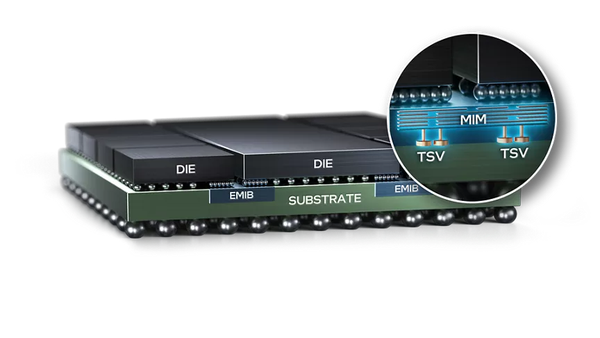
An alternative approach that I personally really like is Intel’s EMIB. CoWoS wastes a lot of silicon. Silicon is expensive and only needed where the data actually has to travel, so why don’t we only use silicon there, and organic substrate everywhere else that doesn’t require these silicon “bridges?”
Meme credit: @Alex_Intel
3D Stacking and Hybrid Bonding (now-future)
If you ever sent your kids to summer camp (or went to camp yourself if you’re Gen Z) you probably understand the idea of bunk beds. By going vertical, you can fit more in the same horizontal space. This is 3D Stacking.
Stack chips directly on top of each other, connected by vertical pillars called Through-Silicon Vias (TSVs). This is how HBM works already, 8 to 16 DRAM dies stacked like a tiny skyscraper, with thousands of TSVs creating a massive memory bandwidth highway.
However, taking this to the world of logic is what is transformative. AMD is already doing something like this with their vertical 3D V-Cache.
There is one futuristic technology that is very necessary for this. It’s the most transformative packaging technology since flip-chip, enabling interconnect densities that were science fiction five years ago.
All packaging today requires some form of bumps or solder balls that melt when heated in order to connect stuff. Hybrid bonding eliminates bumps entirely, directly fusing copper pads between chips.
How? Polish the copper pads and dielectric surfaces so flat they’re atomically smooth.

Then you press them together and the copper atoms literally diffuse across the interface and form a single metallic bond. With Van Der Waals forces.
Why does this matter? Three reasons.
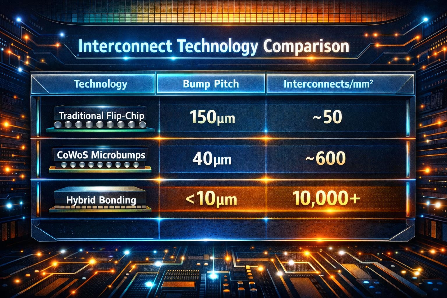
Density: Sub-10μm pitch means 10,000+ interconnects per mm². This is because the solder balls in non-hybrid-bonding packaging techniques are spheres that bulge around the edge, capping how dense they can be packed without touching and shorting each other.
Power: Shorter connections = less energy wasted pushing electrons through bumps. This matters a LOT when you’re stacking logic on logic.
Thermals: No solder bumps means better heat transfer between layers. The underfill problem from flip-chip days gets way more manageable.
However, the surface prep is insanely demanding. It requires sub-nanometer flatness across an entire wafer. One particle and the bond fails.
The Interconnects Are Getting Really Dense
Something cool mathematically happens when you shrink the bump pitch: Interconnect density increases non-linearly. That’s because interconnects are packed in a 2D grid, so density scales with the square of pitch reduction. This is very good for packaging scaling keeping up with the transistors.
And this is why hybrid bonding is soooooooo important. So important.
This was a fun read!
Thanks for the clear explanation. You did great job dumbing it down. Now I finally understand where to focus on to invest.