


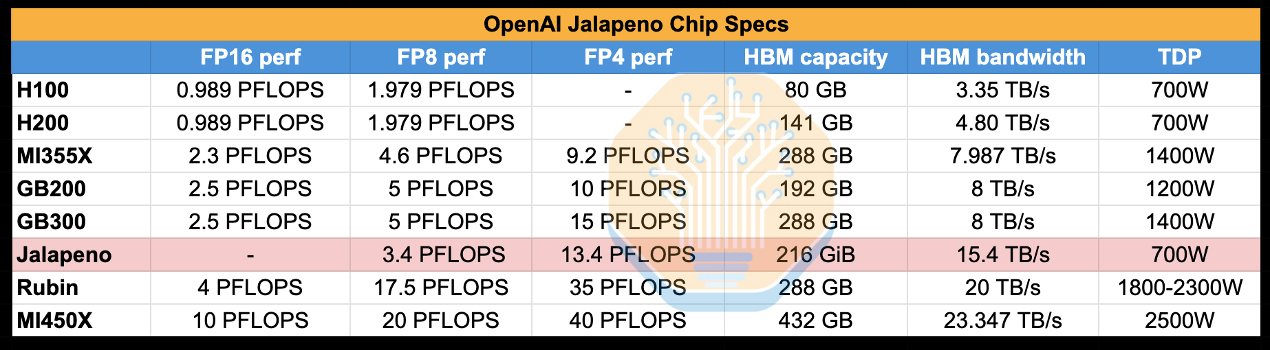
There was some spicy news this morning about a spicy chip from a spicy frontier lab who will be the last presenter today at Hot Chips.
Mamma mia
follow me on on X: x.com/jasonschips
Contents
Samsung LPDDR5X Processing in Memory
XCENA MX1 CXL Computational Memory Device
Thor Ultra: Ethernet NIC Chip
NVIDIA BlueField-4 DPU
NVIDIA Spectrum-X Multiplane Network Architecture
Cerebras CS-4
SambaNova RDU
Google TPU v8
OpenAI Jalapeno
Samsung LPDDR5X Processing in Memory
We have memory themed presentations again today.
Samsung will not stop shilling processing in memory (PIM). Honestly very reasonable. They are really the only ones who can do this and benefit from it.
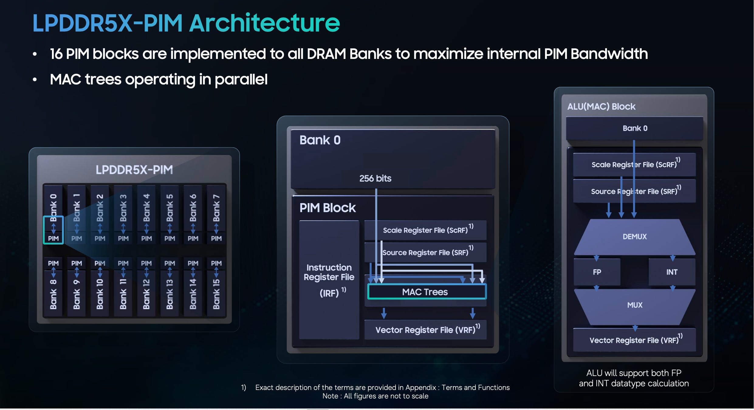
PIM just means a small logic block next to each DRAM memory bank.
It can support 8x the bandwidth of LPDDR5X. If you add processing you can just send only the data that needs to go back to the main processor.
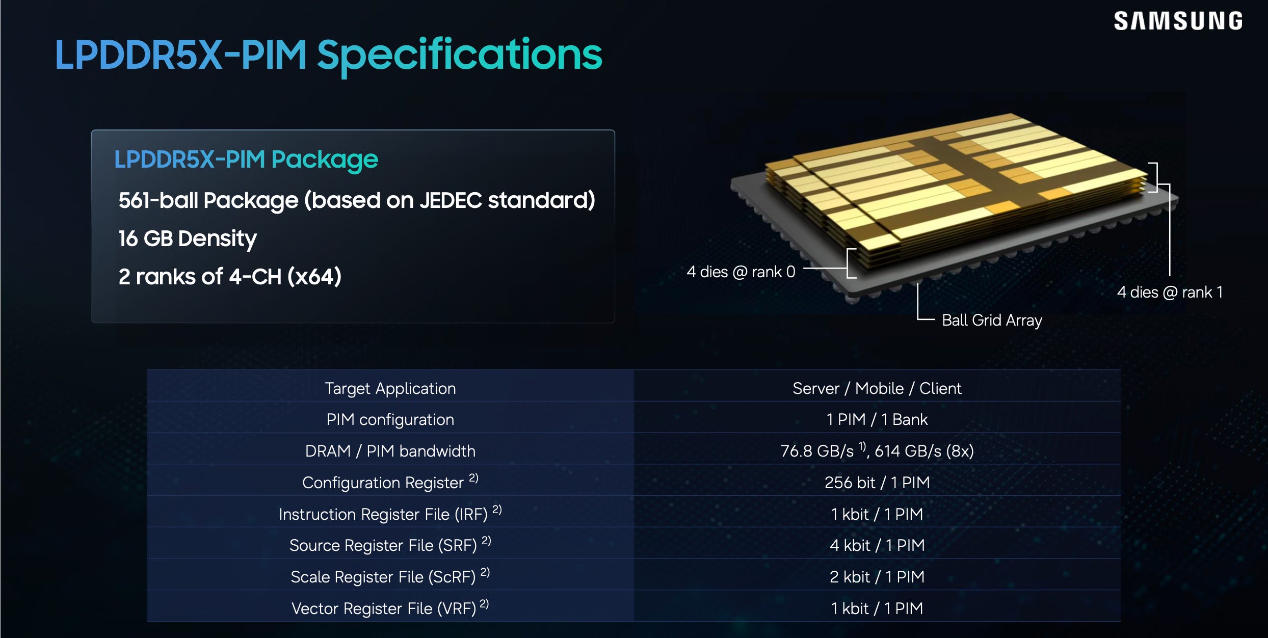
Can apparently be used for both server and edge.
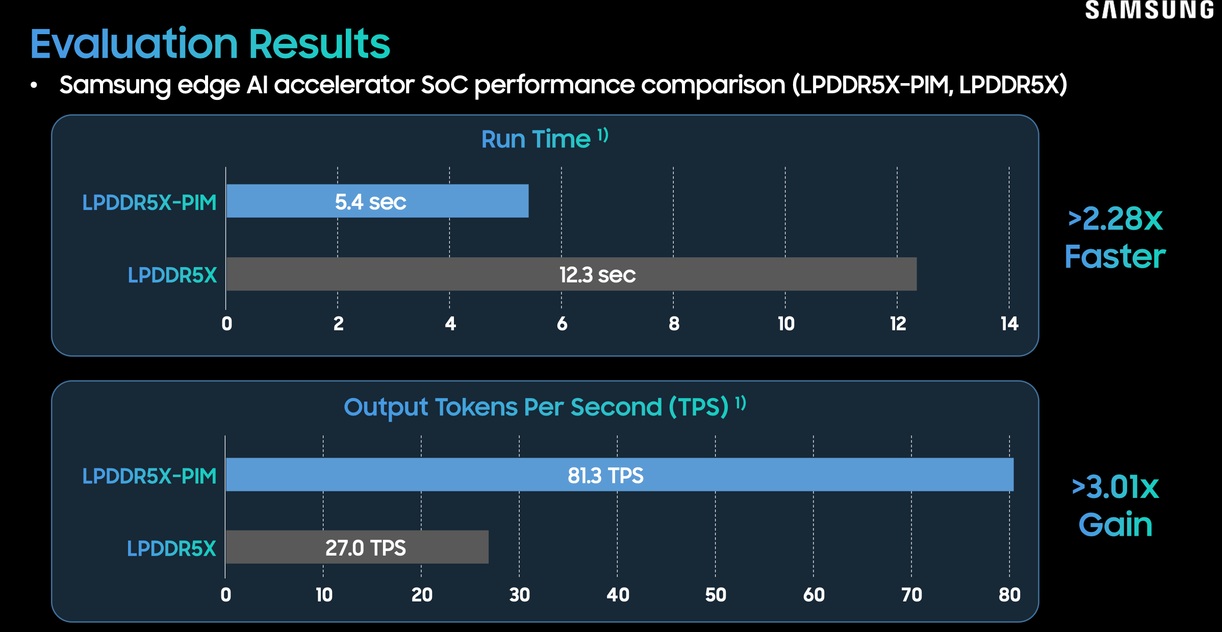
Yeah this is pretty darn cool. Dunno what the actual cost of something like this is from Samsung but you def see the potential.
XCENA MX1 CXL Computational Memory Device
Jointly presented by Samsung as well. CXL is memory pooling that improves utilization of memory and expands memory arbitrarily. SSDs are seen by software as actual memory and DRAM serves as cache. They call it infinite memory for a reason. Generally very bullish for NAND since it invites it to DRAM’s memory tier by solving some of the latency problem.
MX1 is a “memory accelerator” near memory compute chip that enables this stuff. So again, you have Samsung shilling compute with memory. Not PIM but near memory compute and happens to be fabbed by Samsung lol.
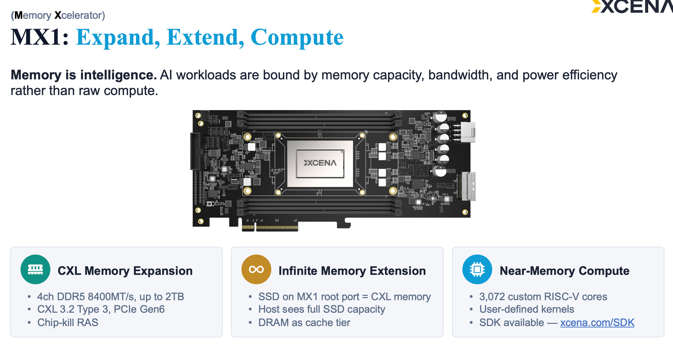
Funny enough they use RISC-V. This is a CPU with many small cores that has nowhere near the TFLOPS of a GPU but is also kinda programmed like a GPU?
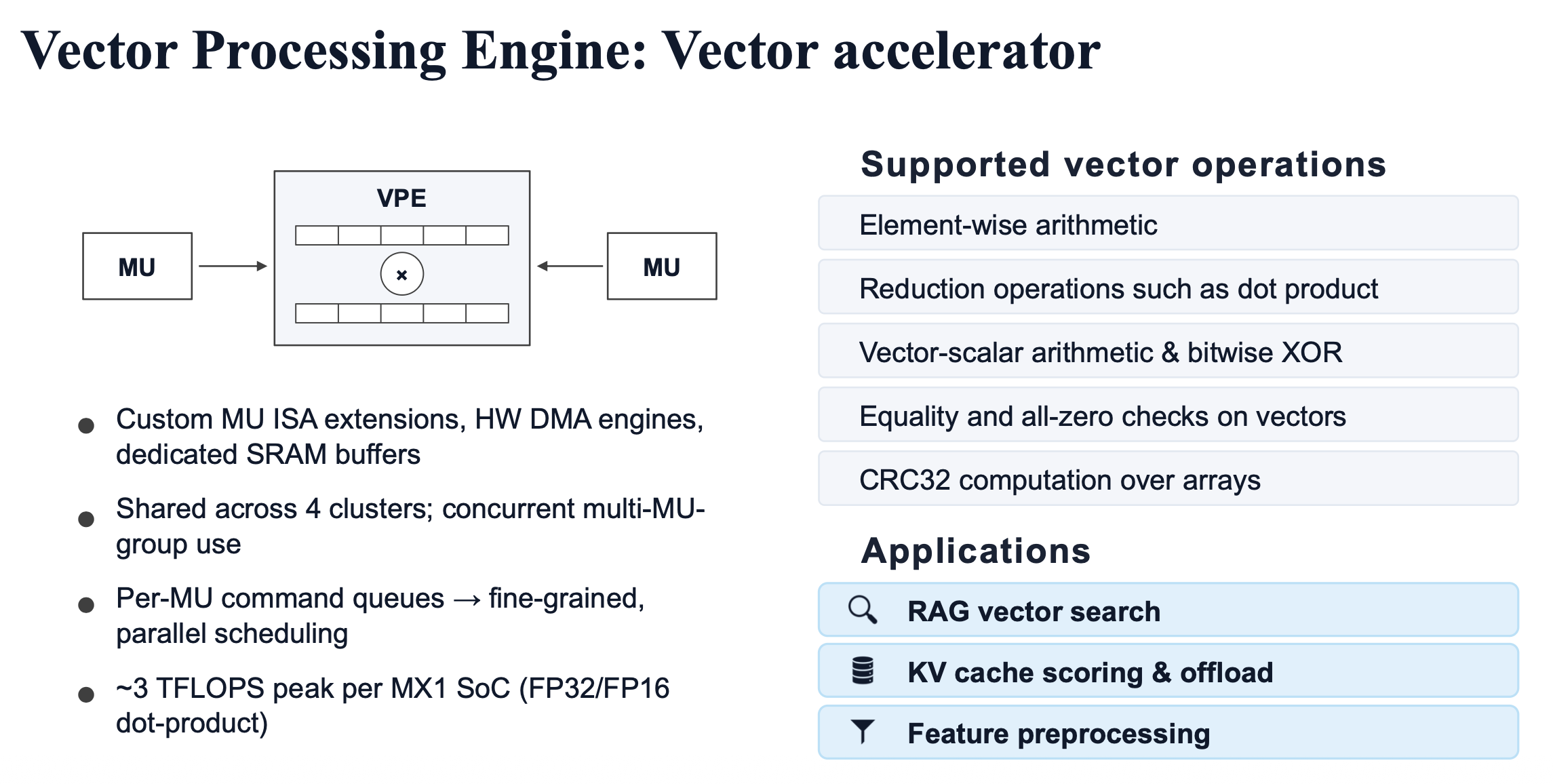
Again, when you have processing near memory you get much higher effective bandwidth.
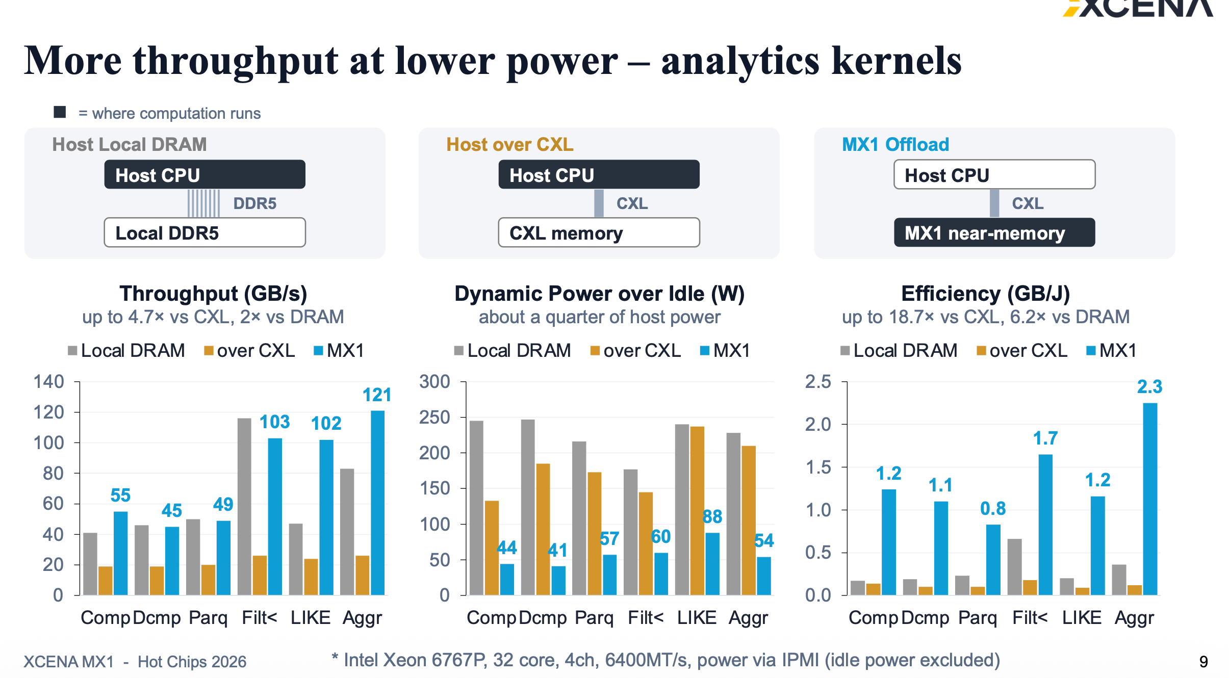
Claudeslop ELI5:
Your files are in the basement.
Local DRAM — filing cabinet beside your desk. Fine, but you can only fit so much there.
Over CXL — you needed more room, so the files moved to the basement. Now every question means carrying boxes up the stairs. Slow, and exhausting.
MX1 — hire someone who lives in the basement, reads the files there, and sends you only the answer.
Broadcom Thor Ultra: Ethernet NIC Chip
Broadcom’s NIC. Network Interface Cards (NICs) allow GPUs to talk directly to the scale-out network without going through a CPU. They use Remote Direct Memory Access (RDMA) to directly access GPU HBM. This is also where the transceiver plugs in.
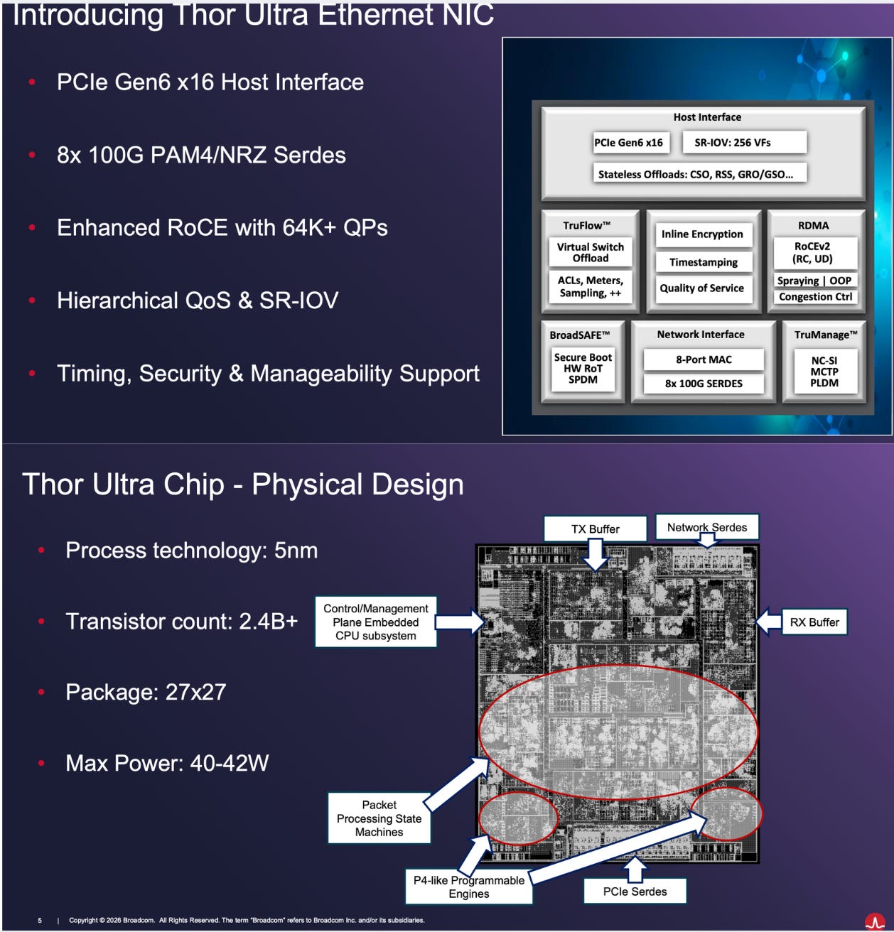
This is the chip.
NVIDIA BlueField-4 DPU
What does a DPU even do? A data processing unit is not a very good name. Think a better name is datacenter processing unit. It is just a CPU that runs the infrastructure software workloads away from the main CPU so it can focus on OS and apps. “Networking, storage, and security.”
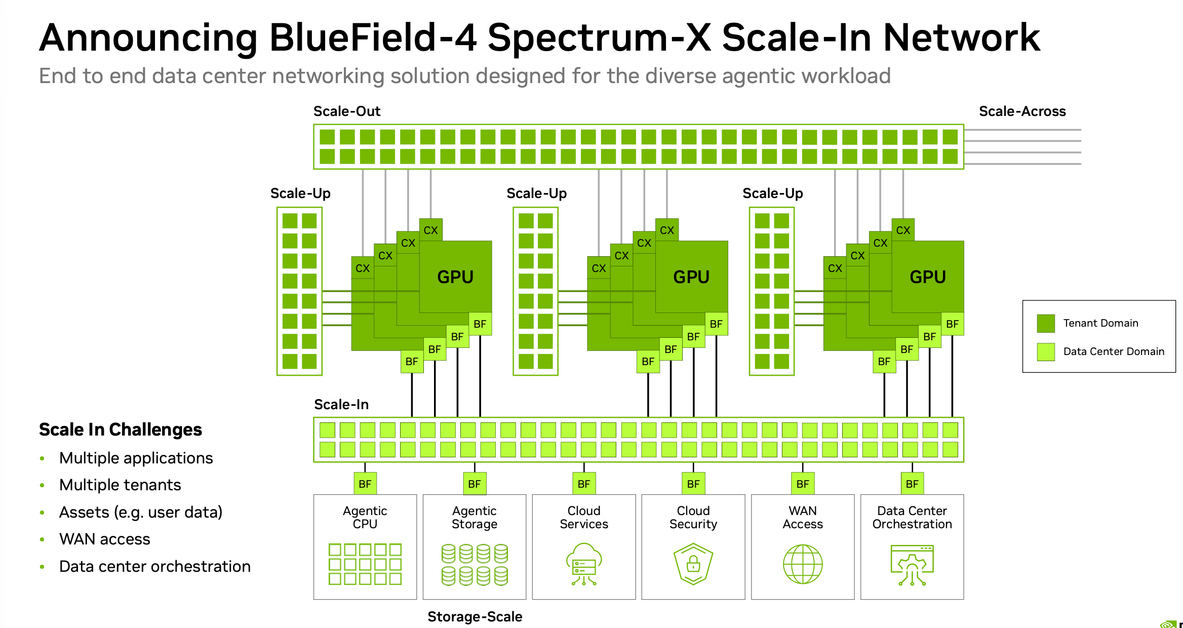
Scale-up, scale-out, and scale-across connects GPUs to each other at varying scales. Scale-in (which uses DPUs) connects GPUs to datacenter resources such as storage and security.
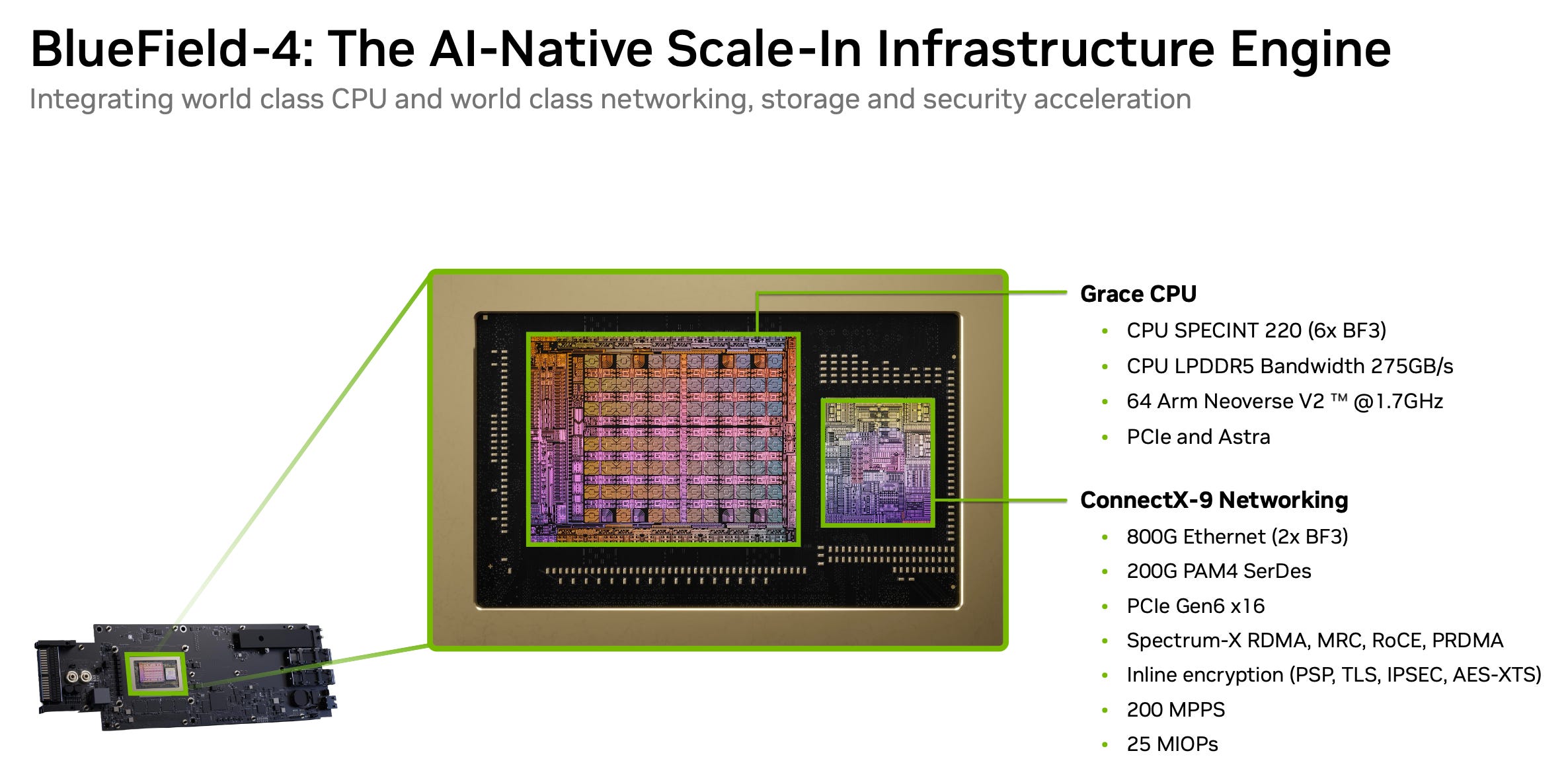
Bluefield 4 is made up of a Grace CPU and a ConnectX-9 NIC. Basically the difference between an AI DPU and traditional cloud DPU is the insane bandwidth. Bluefield 4 has 7.2Tbps.
NVIDIA Spectrum-X Multiplane Network Architecture
Now this is the fun one.
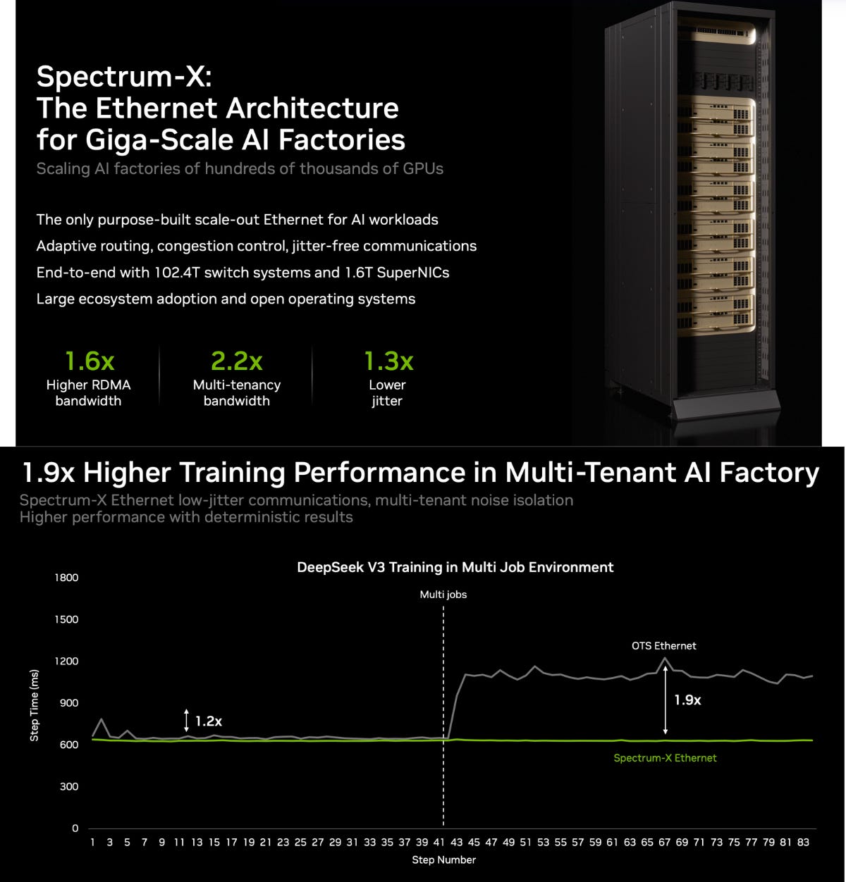
Spectrum-X is Nvidia’s ethernet scale-out. Custom designed for higher bandwidth and lower jitter (variance in latency). Way more popular than Infiniband.
Multi-tenancy is when one fabric handles multiple jobs. Spectrum-X was specifically designed for this and has 1.9x better performance in multi-tenancy.
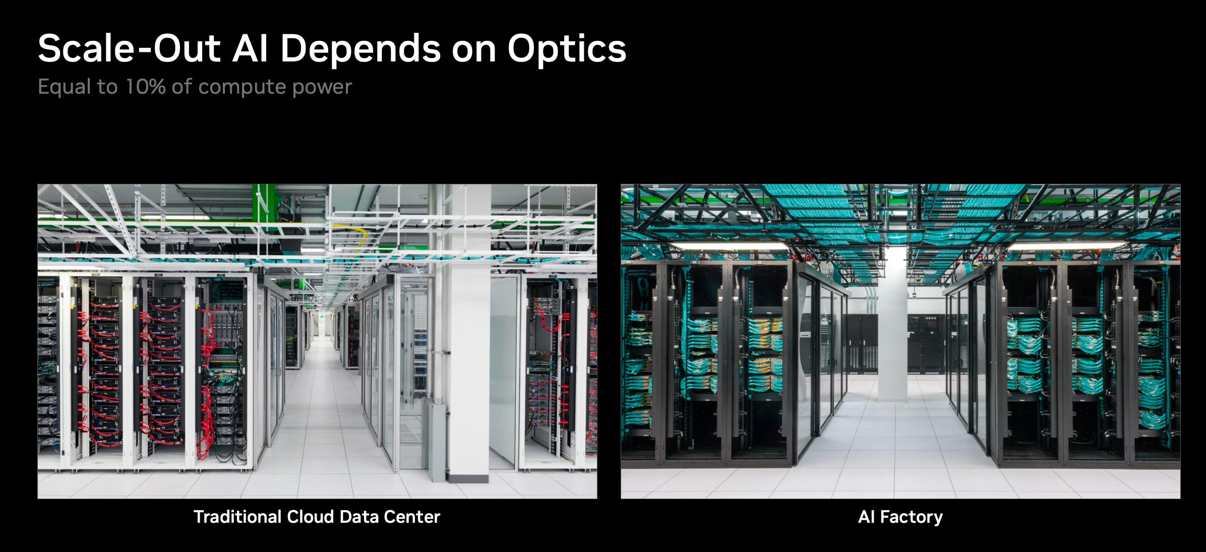
We know why you need CPO for scale-up. But why do you need it for scale-out? It’s already optical.
The answer is power.
CPO low power because you eliminate DSP to correct the degraded signal from the long copper trace to the faceplate because it is co-packaged.
Now onto the main even which is multiplane networking architecture.
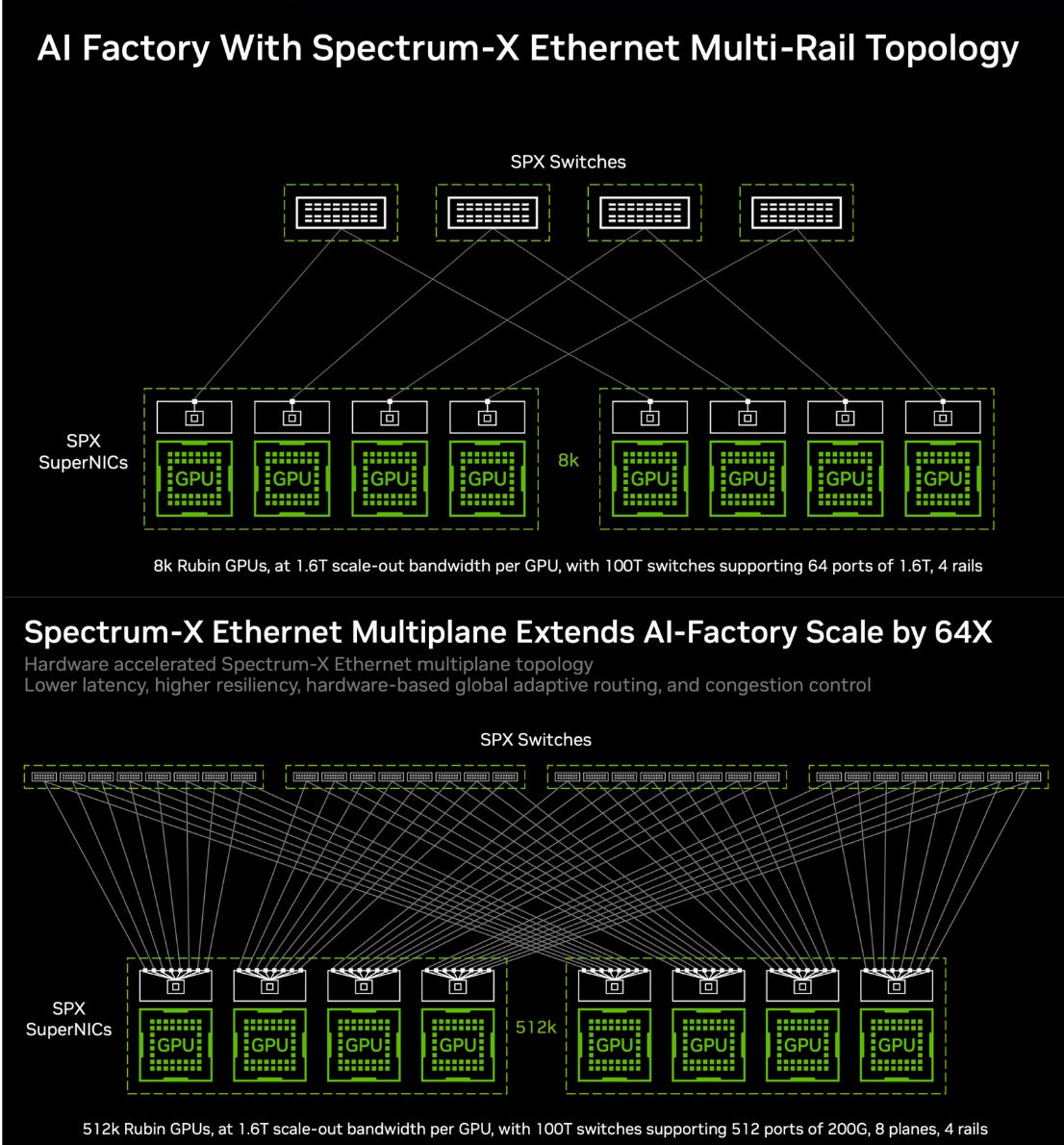
Traditional scale-out is one port per GPU. Say you have 64 1.6T ports on your switch for 102.4 Tpbs total bandwidth (which is what Spectrum-X switch actually has). You can do a neat trick where you have 512 200G ports instead and each GPU gets 8 ports or more specifically access to 8 planes of network, each with one port of 200G.
So what this does is a few things. First, the network becomes WAY more reliable. Second, you need less switches which is bad for optics. 1.7x less to be precise.
Cerebras CS-4
Cerebras doin an announcement
No one cared.

Looooook at our chip! It’s so big
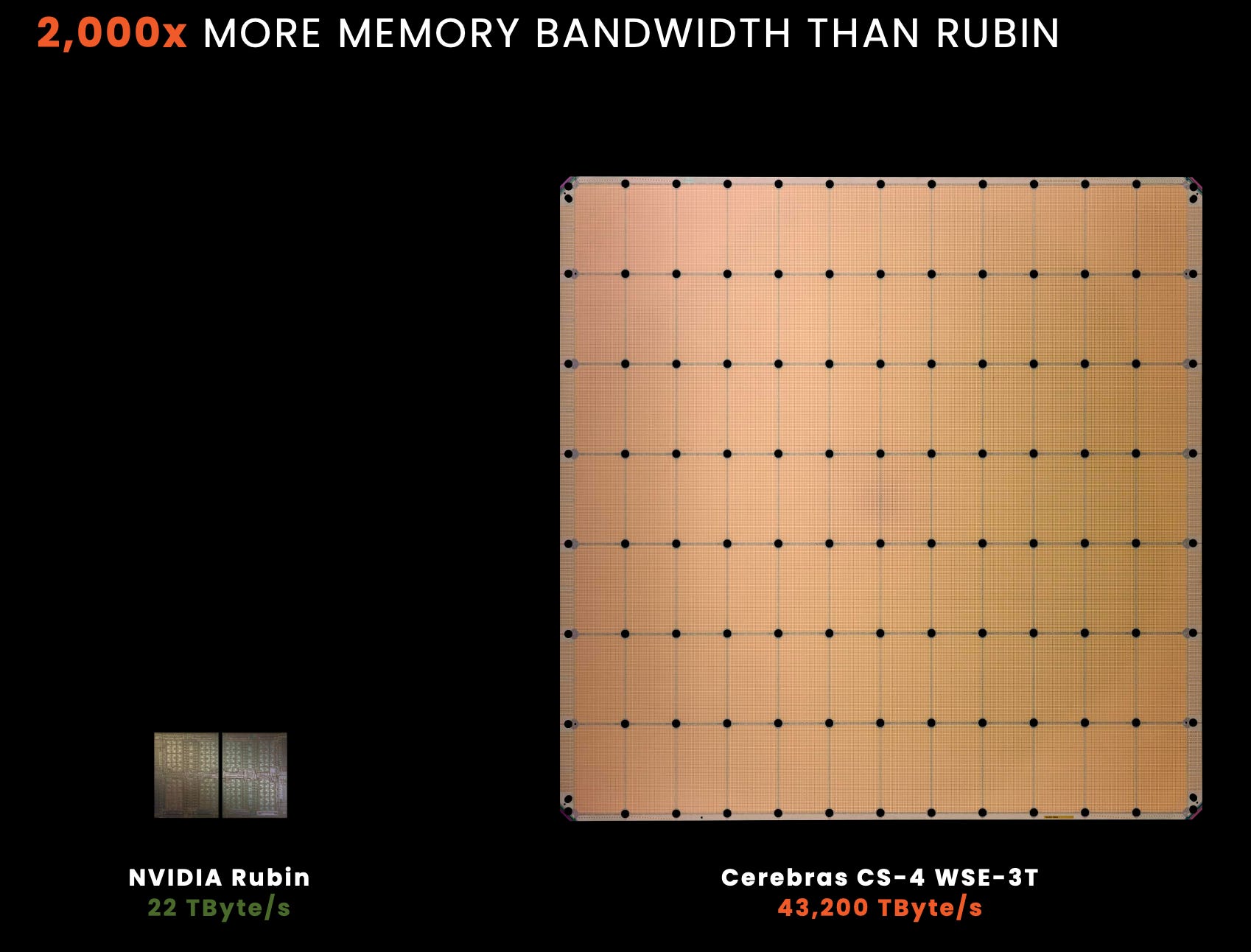
Big chip big improvement.
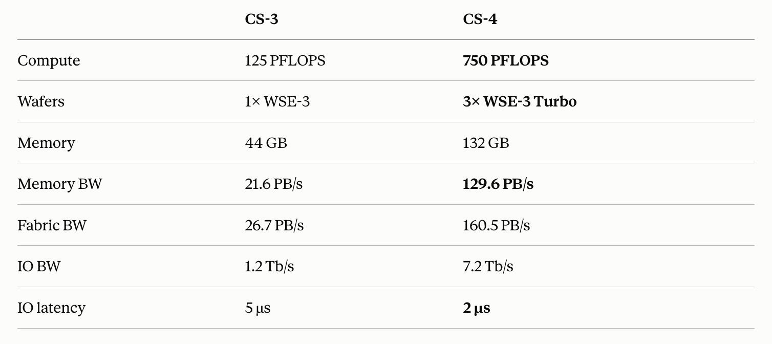
Now with rack that has 3 chip.
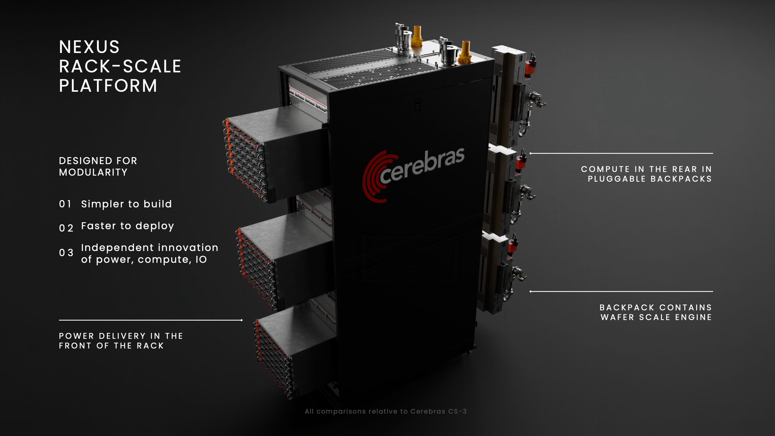
Ok no more slop.
They also announced CS-6, which has hybrid-bonded DRAM on the SRAM wafer. If they can solve the thermal issues associated with this and actually get it to work, they’ll be a huge company. Think about it: insane memory bandwidth, but zero memory capacity. If you solve the capacity problem, the world is in your hands.
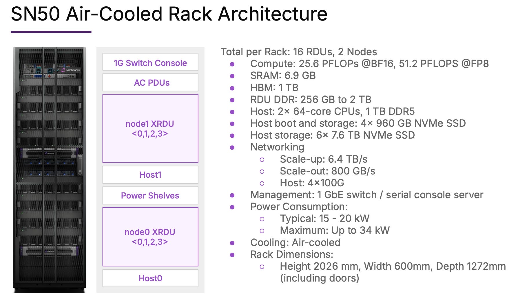
SambaNova SN50 RDU
SambaNova basically says decode is the bottleneck for inference and HBM bandwidth is the bottleneck for decode and most of the HBM bandwidth is spent moving stuff that ain’t weights or KV cache.
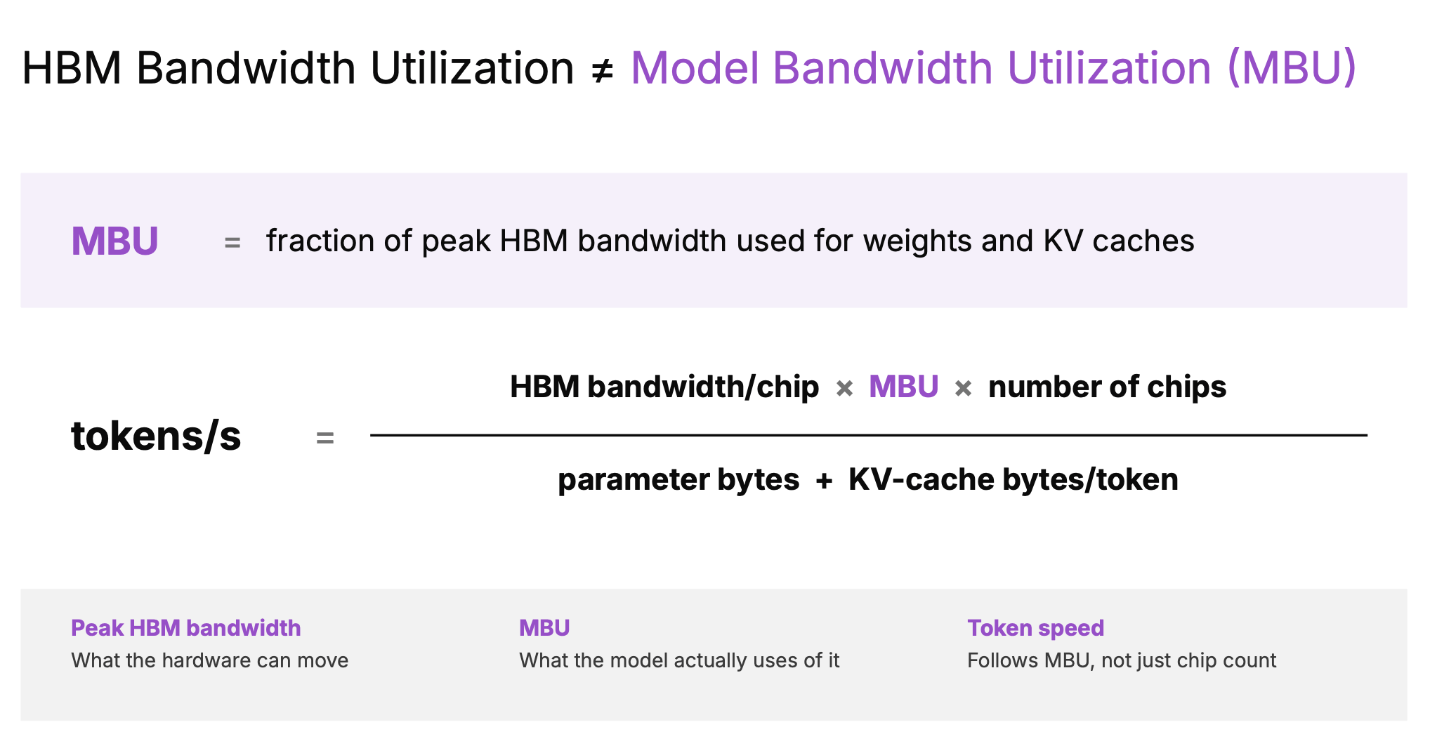
So they built SN50 to be a decode beast. Lots of SRAM and some software/chip design tricks (one kernel for whole model, spatial dataflow).
Google TPU v8
Google’s thing for TPUv8 is making one chip for training and one chip for inference.
TPU 8t and TPU 8i. Can you tell which is which?
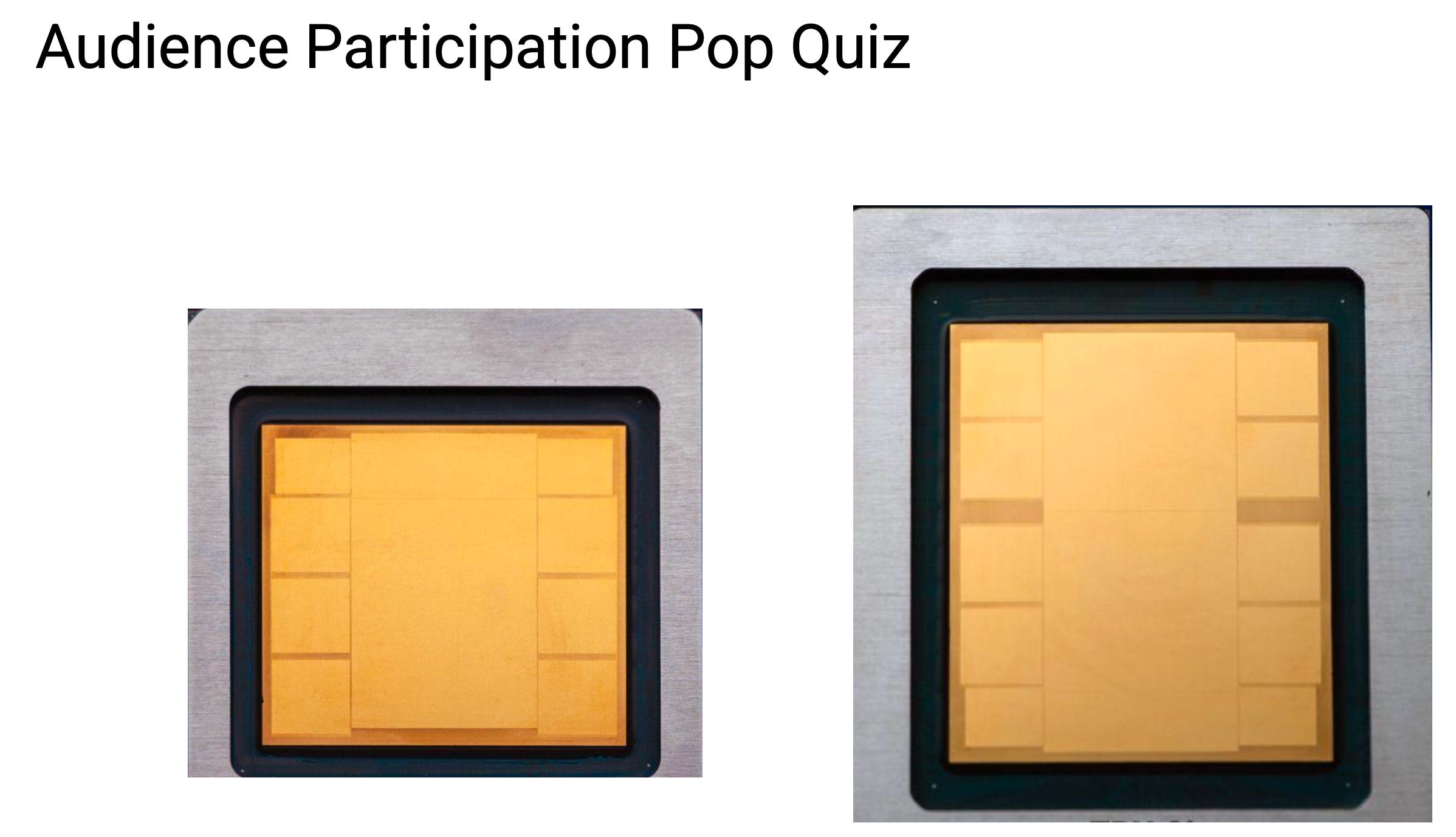
Hint: Inference need more HBM bandwidth per unit of compute because decodeeeee.
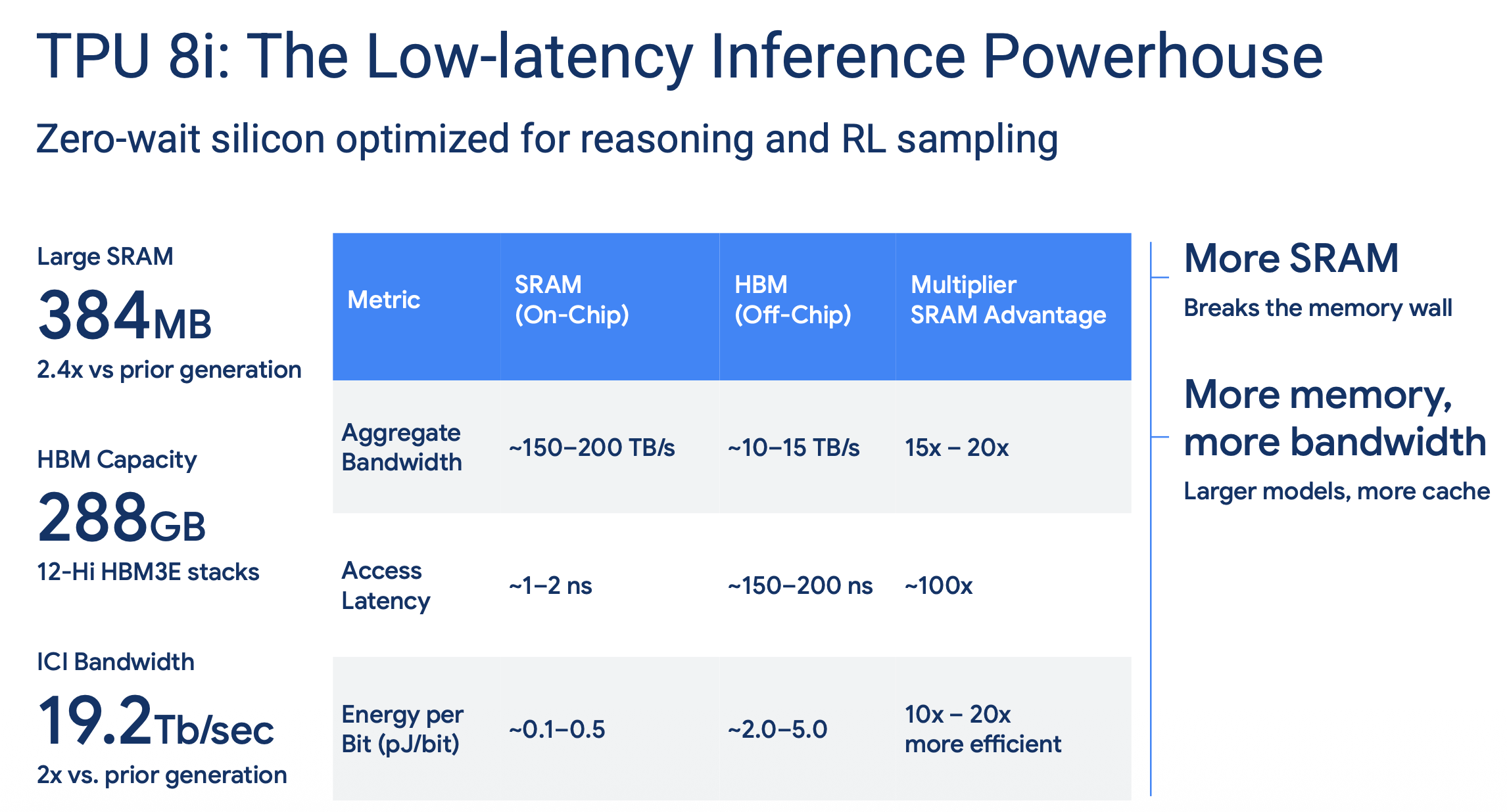
Also lots of SRAM because memory bandwidth.
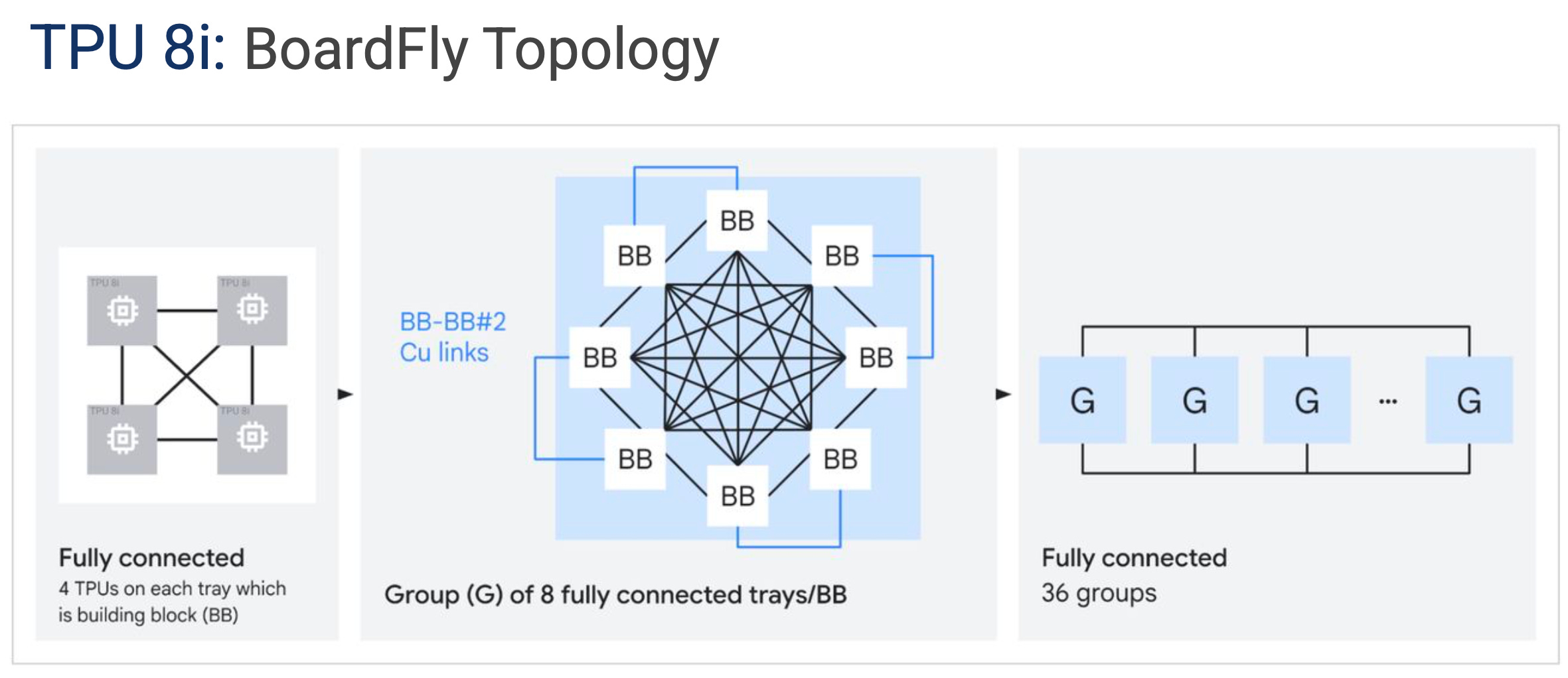
Look at their networking topology. This is to minimize hops to minimize latency.
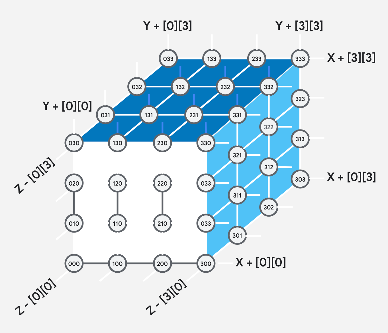
In training you need lots of bisection bandwidth so 3D torus still used. Lots of OCS.
Training needs lots of FLOPS and lots of shared memory.
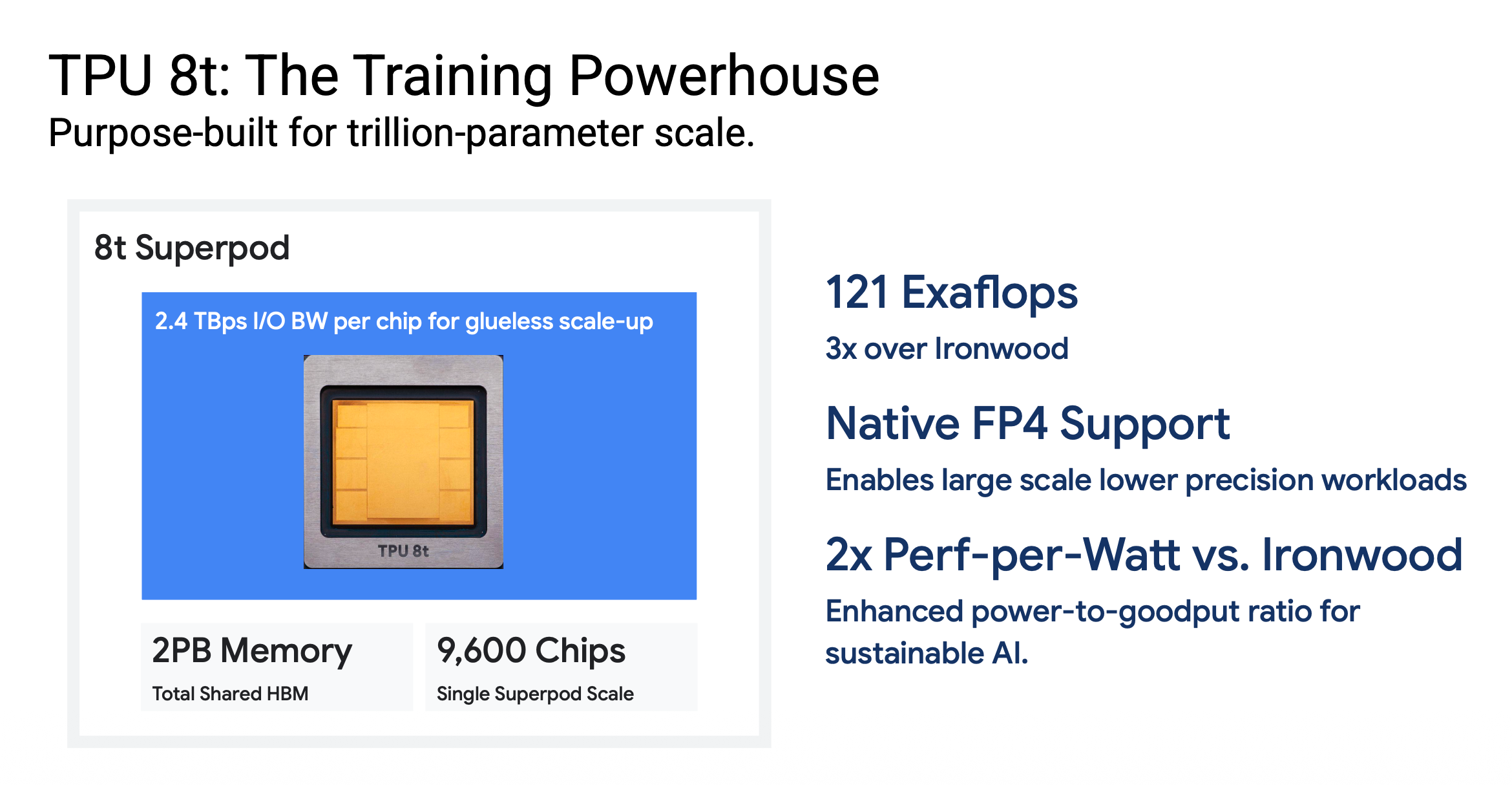
9,600 all-reduce scale-up domain 2PB total memory as typical of Google.
OpenAI Jalapeno
Last and VERY CERTAINLY not least.


They taped out in 9 months. Apparently an extremely small team too. And one of the first things they said was ASTRA helped them build this thing. No chip design experience! Let’s think about what this means for the moats in the space.
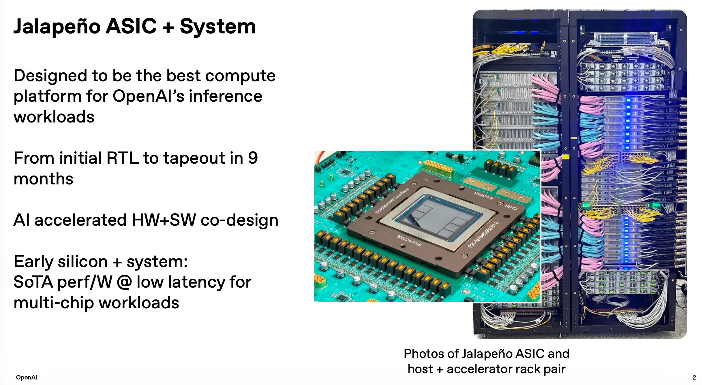
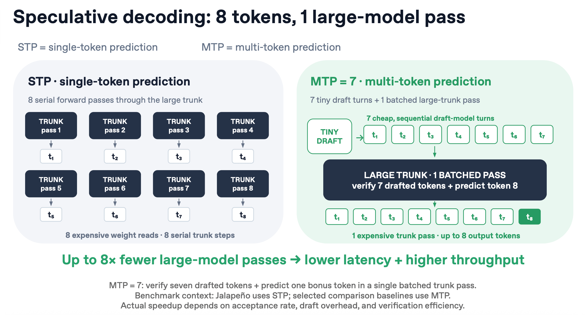
It was designed for speculative decode which is using a cheap draft model to predict several tokens ahead and then check with the main model.
They built this thing for both prefill and decode and for both throughput and interactivity. Trying to be the pareto frontier everywhere.
THIS IS REALLY IMPRESSIVE.
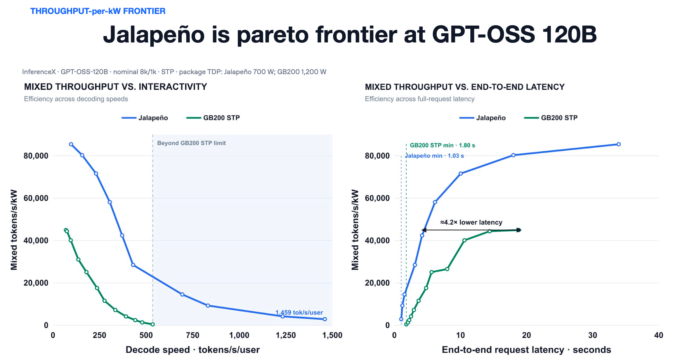
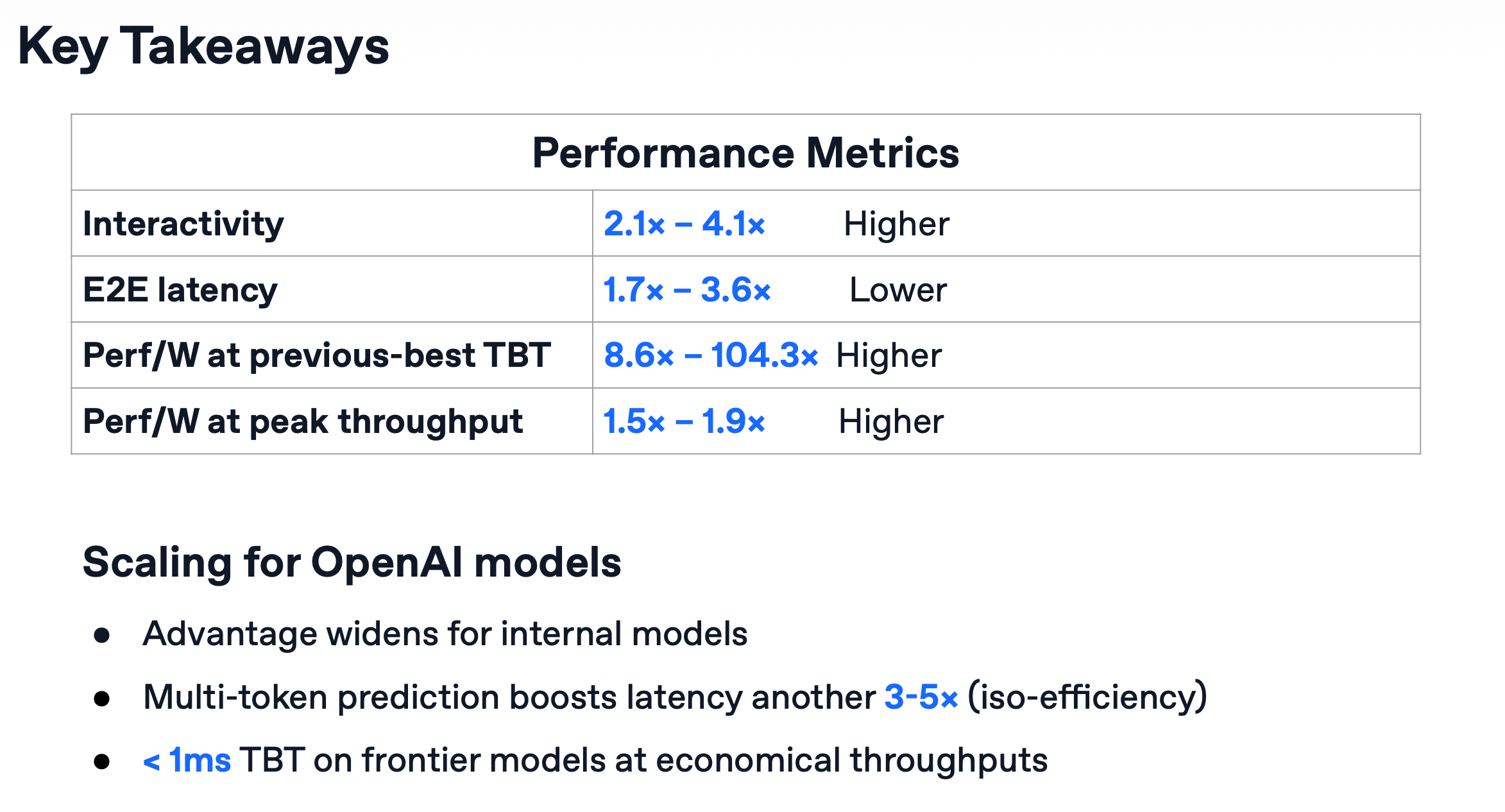
Much bigger improvement on high interactivity side rather than high throughput.
They have 128 jalapenos in a rack with over 1PB of total memory bandwidth (similar to VR200 NVL72).
But the smartest thing they did has nothing to do with the chip itself. It’s their process.
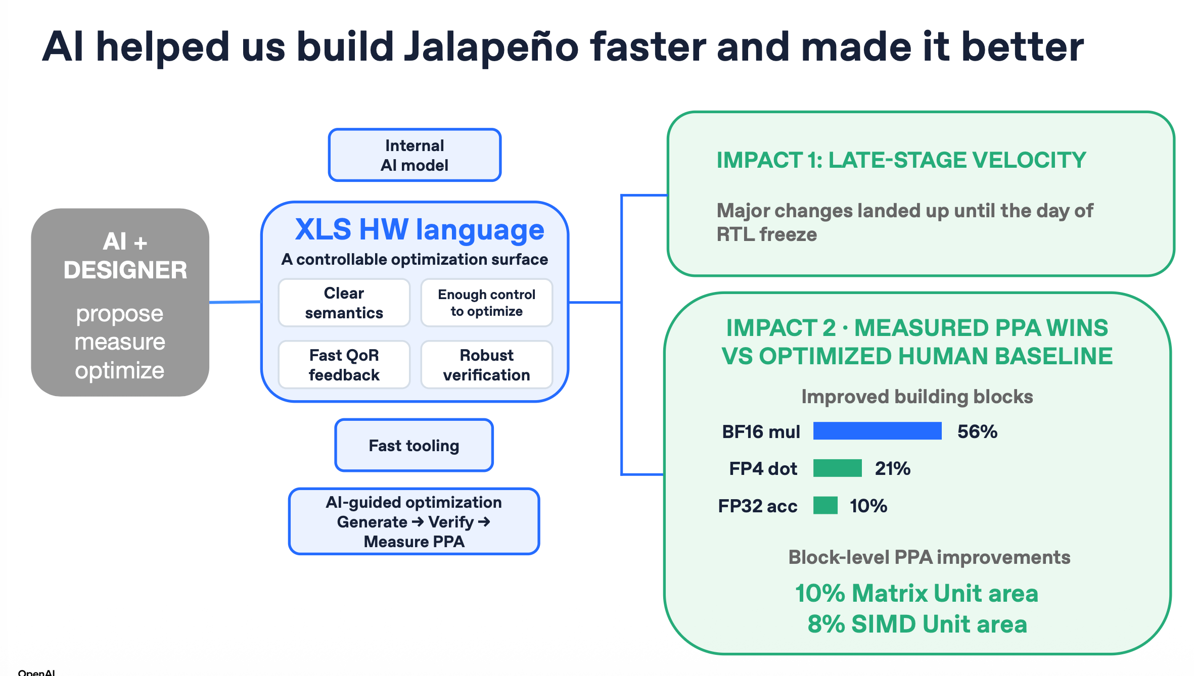
They took a tiny team and had them move fast which I think everyone agrees is better than bloat. But most importantly, they made a new hardware language (!!!) which is kinda similar to Rust so AIs could write correct code out of the box.
But over the long term I think this is pretty bearish any fabless chip designer. This feels like how chip design SHOULD be done. Like with software you are bound to be disrupted if you’re a giant corpo with 2000 engineers and some 19-year-olds can vibe code your shi, as that is how SWE should be conducted. Small, pilled, AI-native team with chip design harness and custom language can easily disrupt the industry. And maybe the giants have the talent today but talent can always be poached…
follow me on on X: x.com/jasonschips