


Hot Chips is indeed hot.
Fun fact: Stanford dorms have no AC. Stanford offers student housing to Hot Chips attendees, so I am staying in the dorms for the duration of the conference. However, what I didn’t know is that for whatever reason this academic institution with a $50b endowment has no air conditioning. So I have been getting really hot during Hot Chips. It’s kind of hard to write when you’re overheating.
Today’s session is all about processing units (PUs). Both the central (C) and graphics (G) kind. This somehow turned out very LONG.
Contents
IBM Z & LinuxONE Processor CPU
Intel Core Series 3 Wildcat Lake CPU
Nvidia Vera CPU
FUJITSU-MONAKA Arm-based CPU
ARM AGI CPU
Intel Diamond Rapids CPU
NVIDIA Rubin GPU
AMD Instinct MI400
Intel Crescent Island GPU
IBM Z & LinuxONE Processor CPU
I was late and joined in the middle of this and had no idea what was going on but I will still cover this.
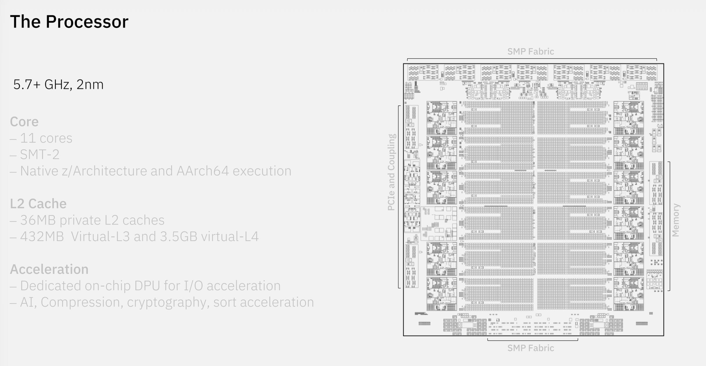
IBM is getting into the CPU game! They are making ARM CPU. Well it is actually dual ISA and executes both z/Architecture and Arm v9.3 natively, in hardware, on the same core. Apparently very high single-core performance for an ARM CPU. Very next-gen so not happening anytime soon. Sort of like ARM AGI?
Intel Core Series 3 Wildcat Lake CPU

This is a chip for computers. Not the ones that are racked up inside datacenters, the ones that actually go on your desk. This is a chip that was already released earlier this year.
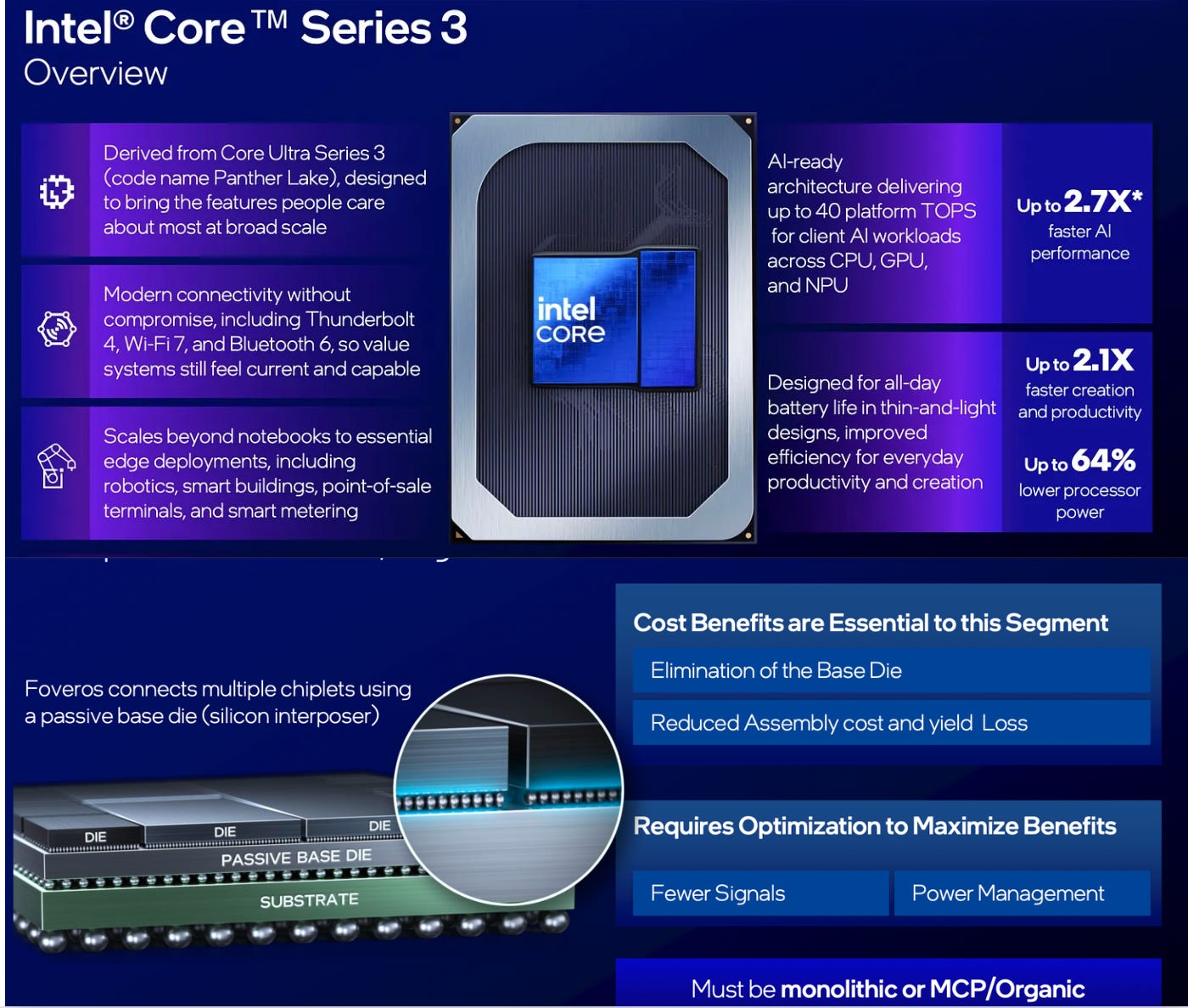
It is an ultra-series architecture for their entry tier chip. Fabbed on 18A. Packaged using Foveros in this chiplet on silicon interposer-like architecture. I personally am not that interested in non-AI-DC stuff.
Nvidia Vera CPU
The first really interesting and directly AI stonk relevant presentation.
Nvidia presentation slides are so Nvidia. Many Nvidia-isms.
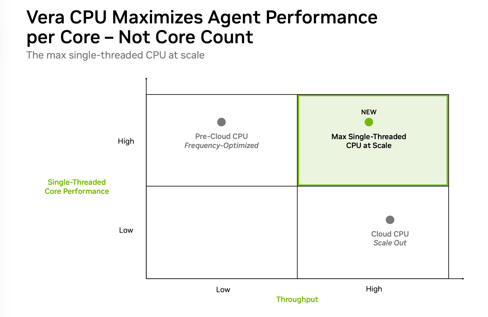
The core pitch for Vera CPU is maximal single-thread performance. This is the bet that agentic workloads need minimal latency and don’t care too much about throughput like desktop multitasking.
Speeding up common agent shenanigans like headless browser use.
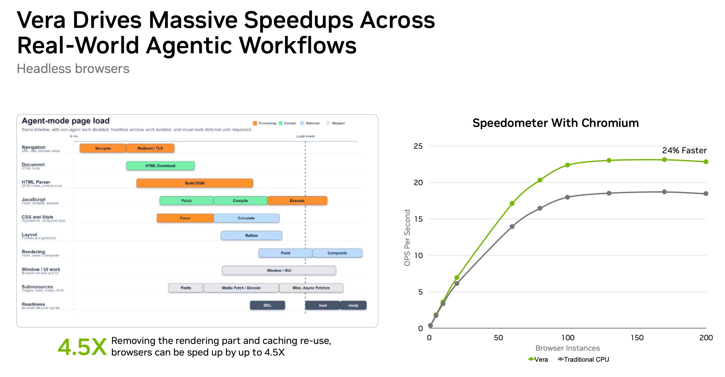
Therefore the tradeoff is simply to make a BIG CORE.
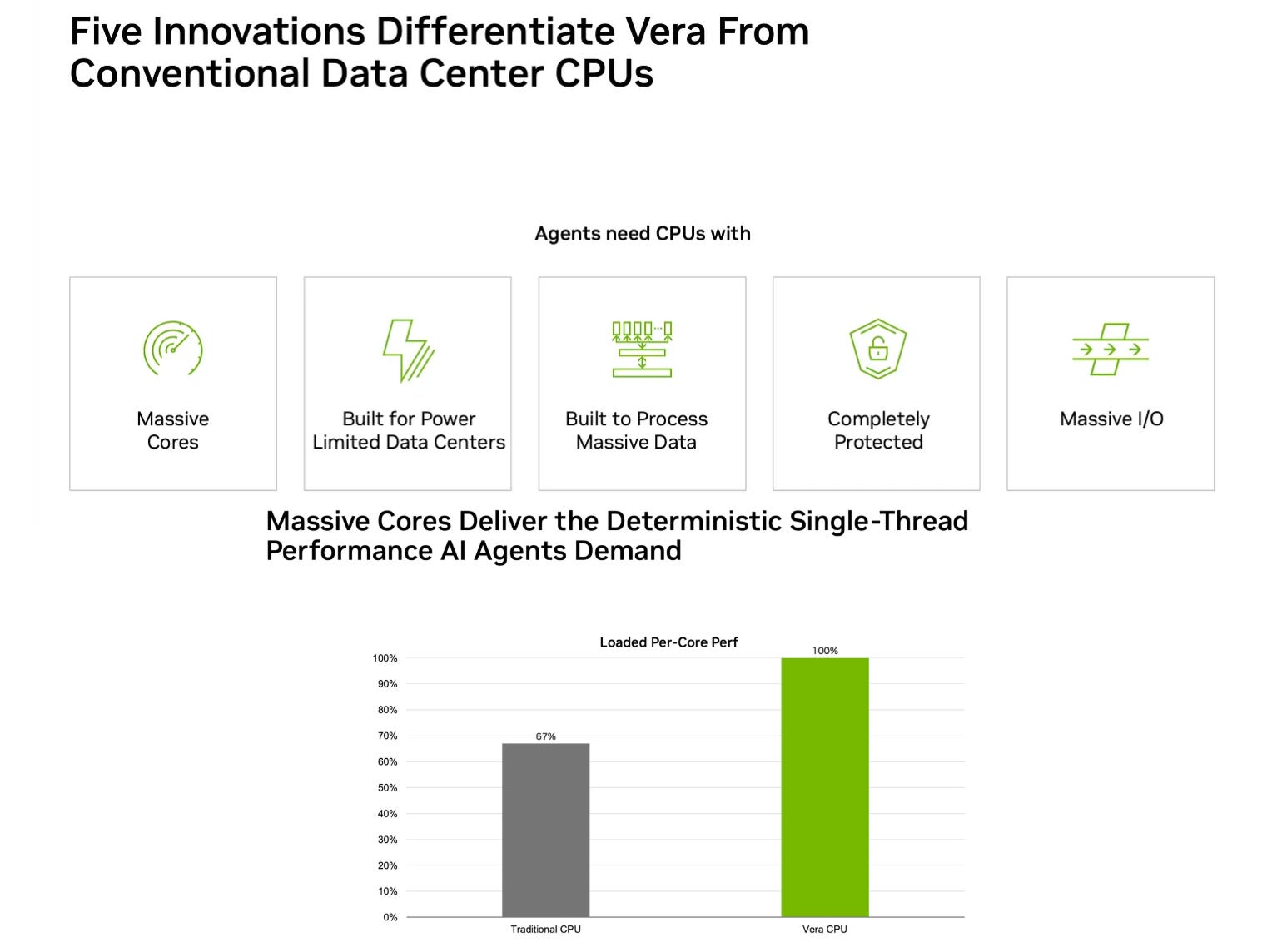
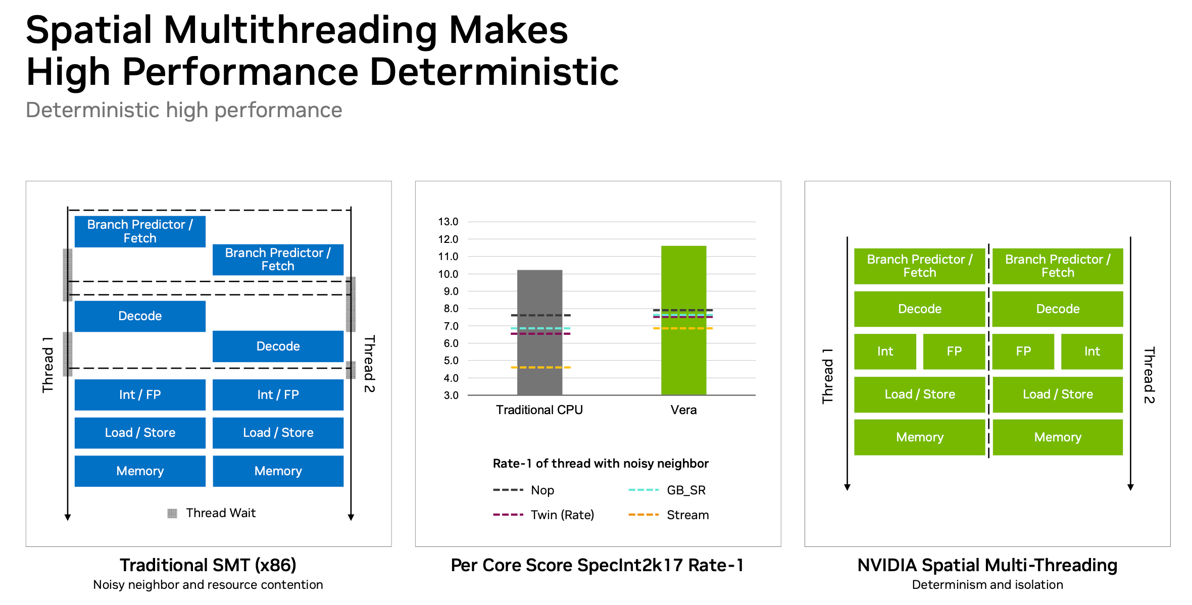
They have a type of multi-threading (multiple instructions on one core) that is not SMT (“traditional” simultaneous multi-threading) called spatial multi-threading (coincidentally also SMT). Spatial just means the threads sort of use different resources and are segregated so it’s deterministic and gives you better single-thread performance. That’s what you get with big core.
They also designed for power efficiency with lower power cores and LPDDR5X.
The thing is built out of 6 dies. The big central die is the massive Olympus cores.
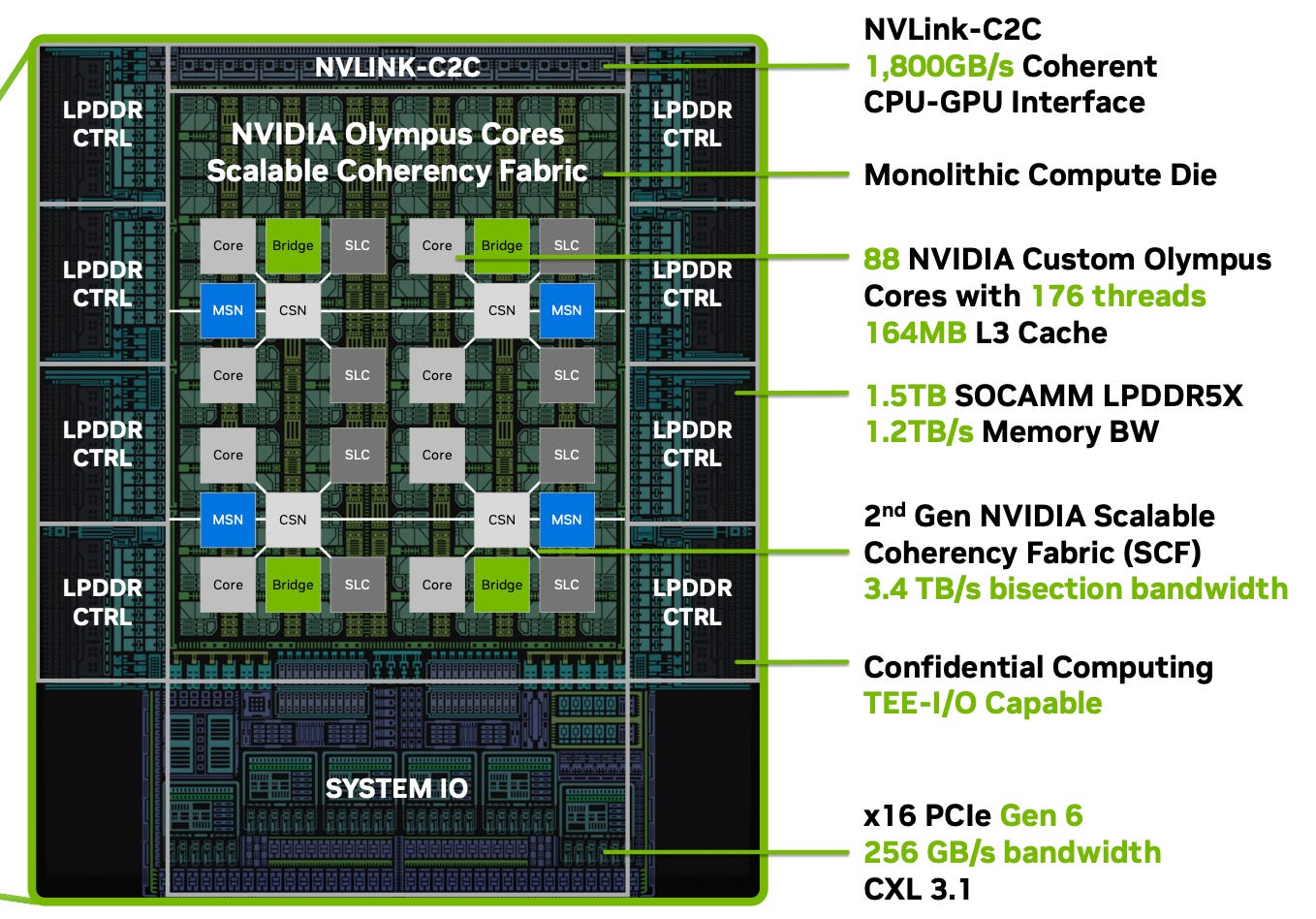
But alas, there are always tradeoffs. There is no free lunch. You have to look at what specs they presented and what they left out, and compare it to AMD EPYC and AWS Graviton.
SMT is statistically more efficient so you’re trading absolute performance/reliability with overall efficiency. It also requires more area. So Vera has like 1/2 the total cores of an EPYC or Graviton.
LPDDR5X is lower power but it is also soldered which means capacity ceilings vs socketed DIMM and worse serviceability.
FUJITSU-MONAKA Arm-based CPU
This is a Japanese company tryna do CPU.
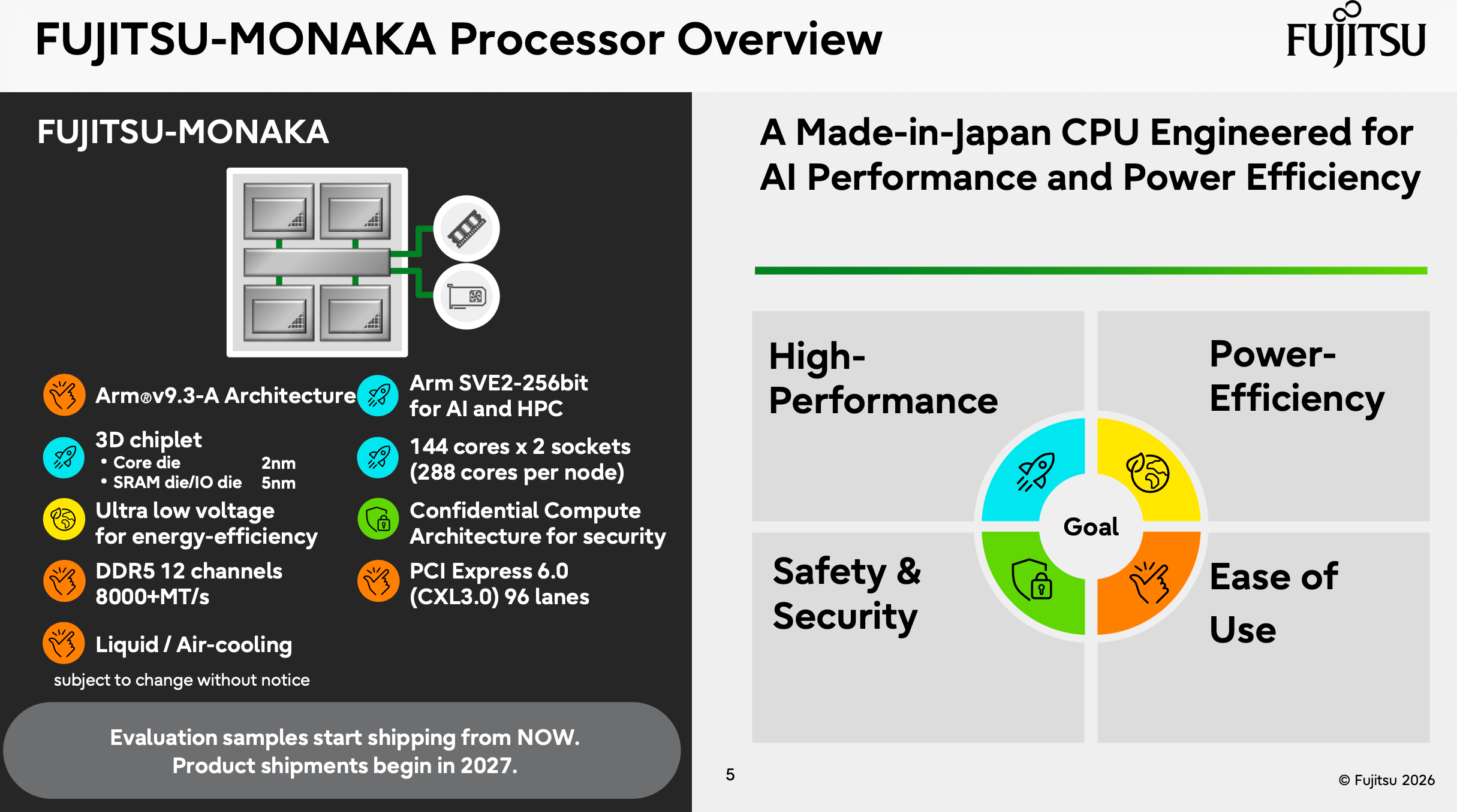
Their core pitch is not using N2 for everything and instead splitting it as N2 for core die and 5nm for SRAM and IO and connecting the chiplets via hybrid bonding.
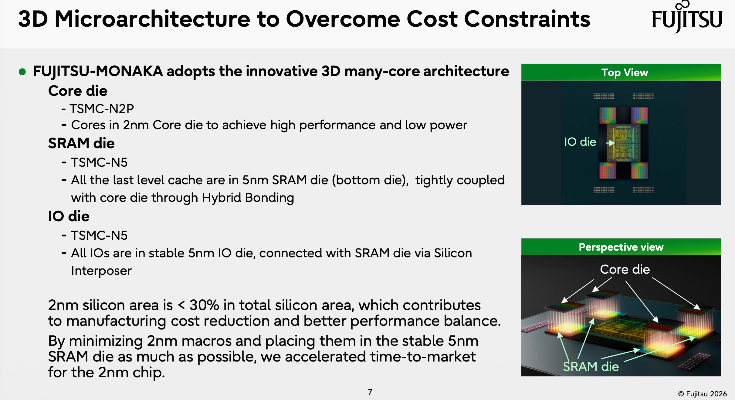
Apparently this optimizes for cost and power consumption.
But also, core dies on the opposite sides of the chip?? This raises an interesting question about core-to-core latency.
Anyways the TLDR is cheap Japanese chip.
ARM AGI CPU
ARM makin’ a chip for the first time instead of just licensing stuff. Before you can use their Neoverse cores for your own stuff (but people don’t like Neoverse for some reason). So they’re using their own IP to make their own chip. This is not new it was announced in the spring and people talked about it a lot then forgot about it.
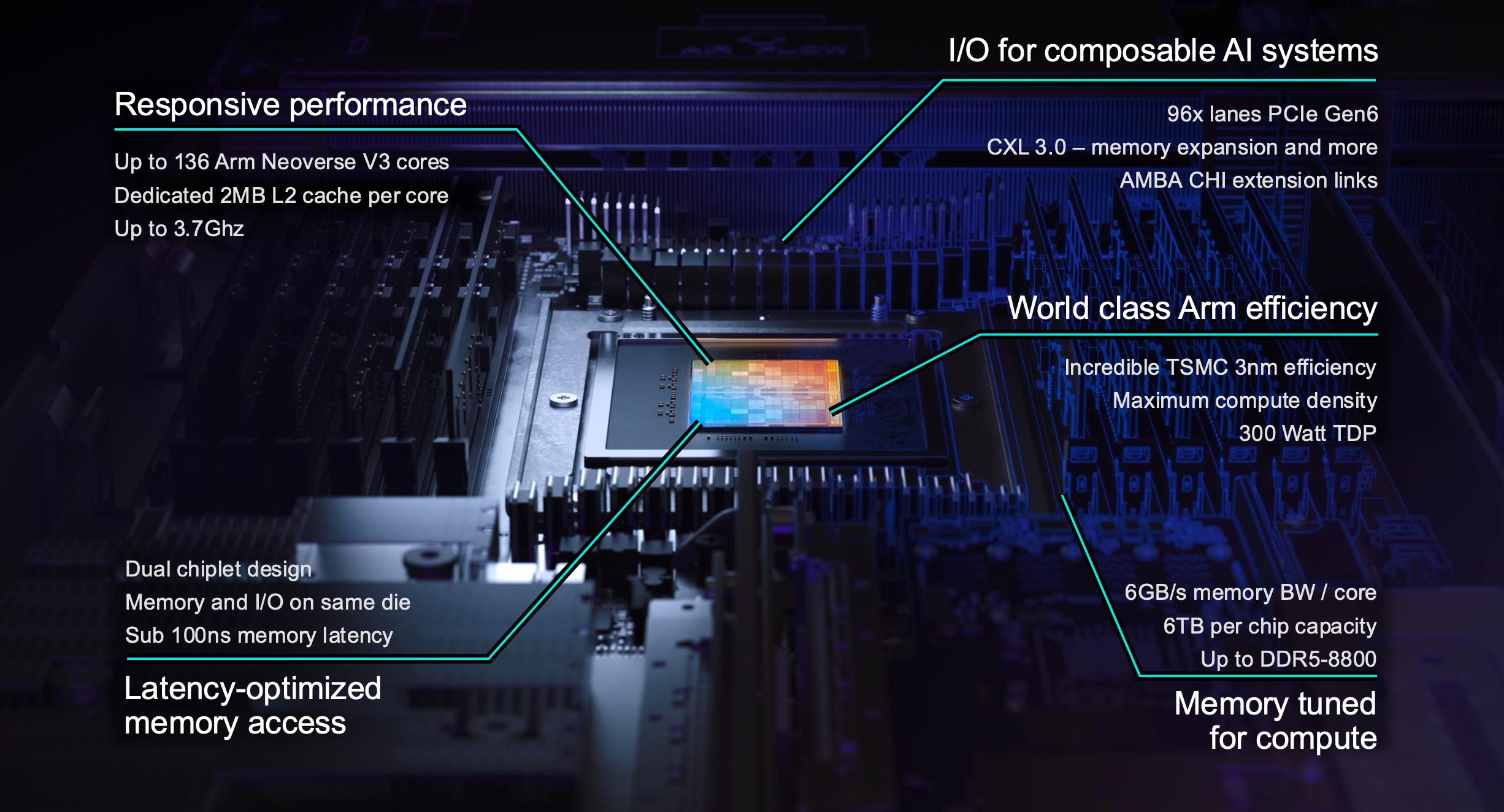
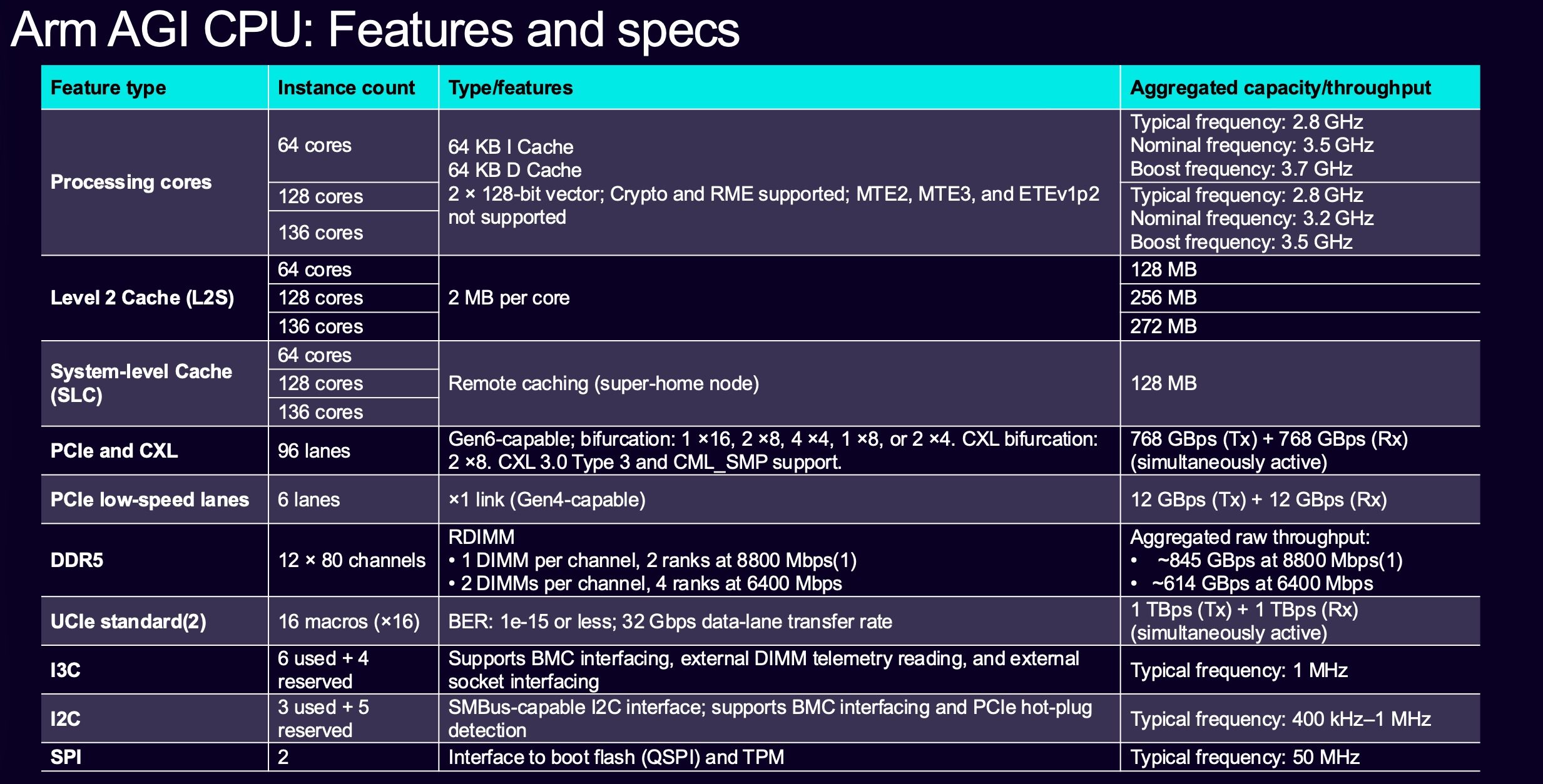
Depending on whether or not you like ARM, you can call this chip balanced (or boring), pragmatic (or unremarkable), and well-rounded (or mid). They are not taking a view on the market like Intel or Nvidia. The more important takeaway is that they are making a chip in the first place.
Intel Diamond Rapids CPU

They are using this fan-out fabric architecture. Basically a bunch of compute “building blocks” surrounding a central I/O and memory “fabric hub”.
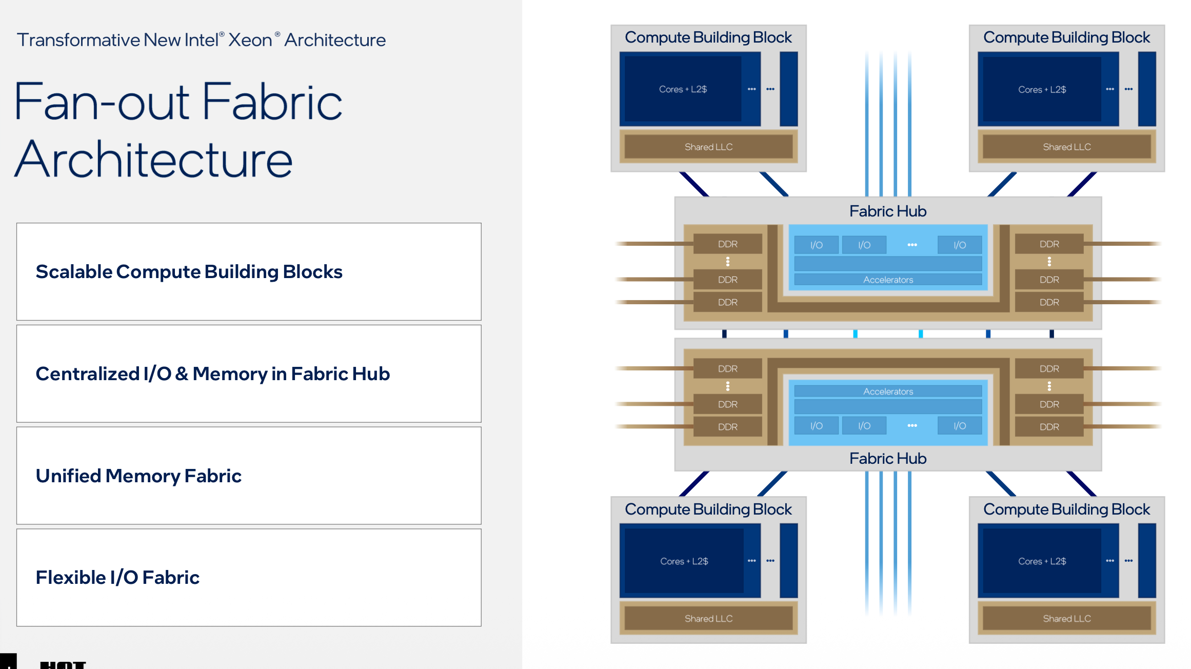
It is very scalable because you can add more compute building blocks to one chip.
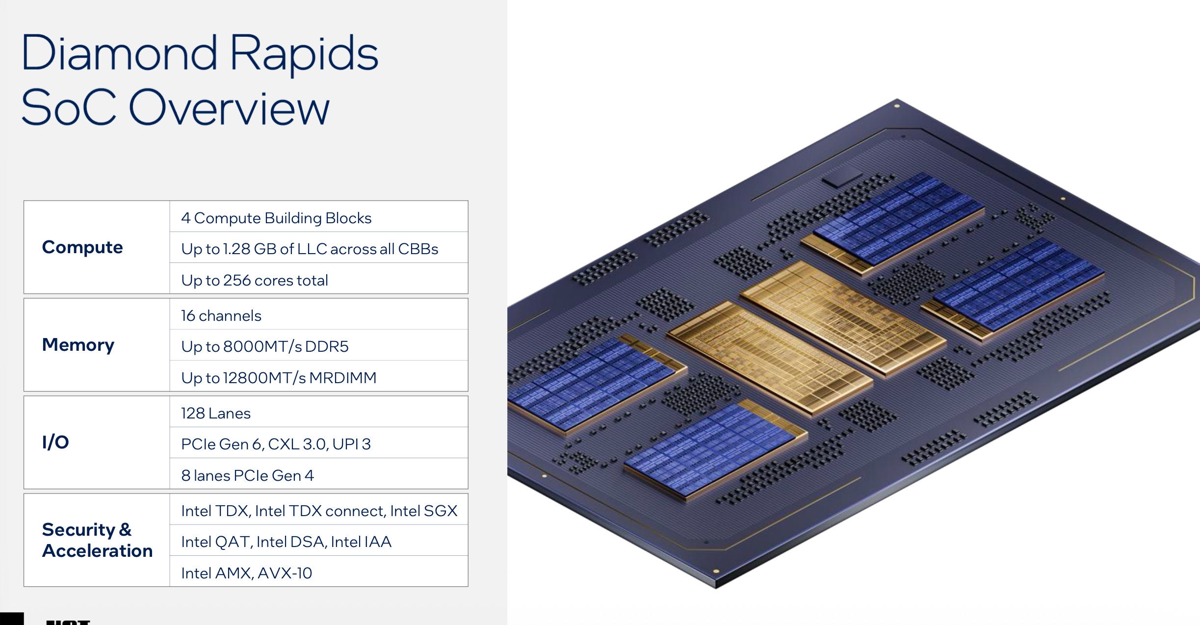
As a result you get an unhinged amount of cache (1.28GB), cores (256), and threads (512).
This is 3x the cores of Vera (88) and more than EPYC/Graviton (192). For cache it is 5 MB of LLC per core vs Arm AGI at 2.9MB, Vera 1.9MB, Graviton5 0.94MB.
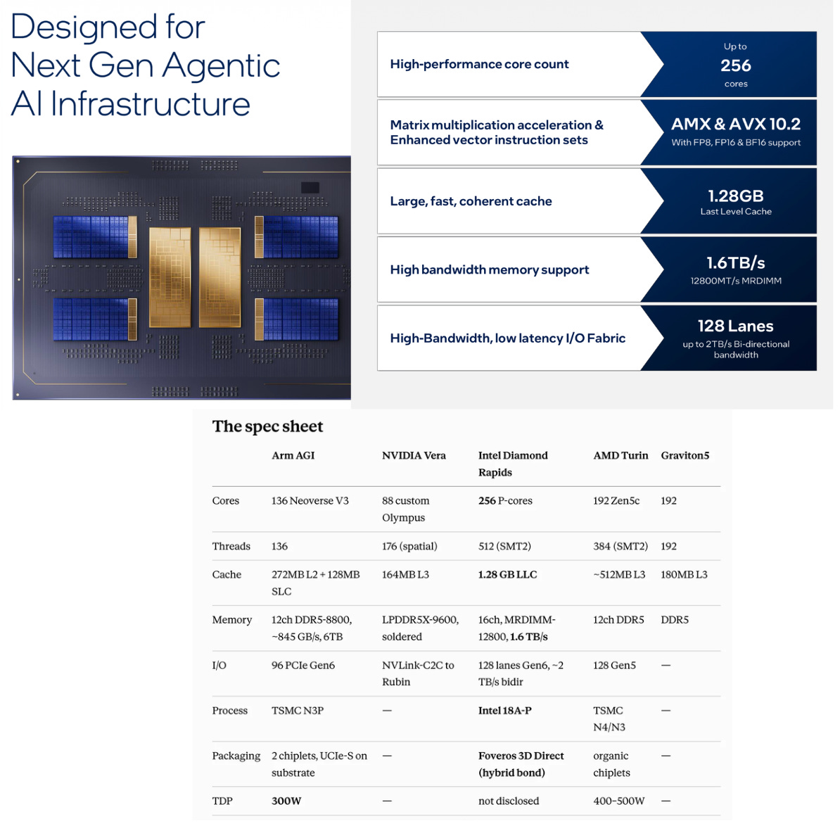
This chip is the polar opposite of Vera. Intel is most definitely taking a view on the market. But it’s not like they say it is for another workload. It is for agentic too! They just shill different specs.
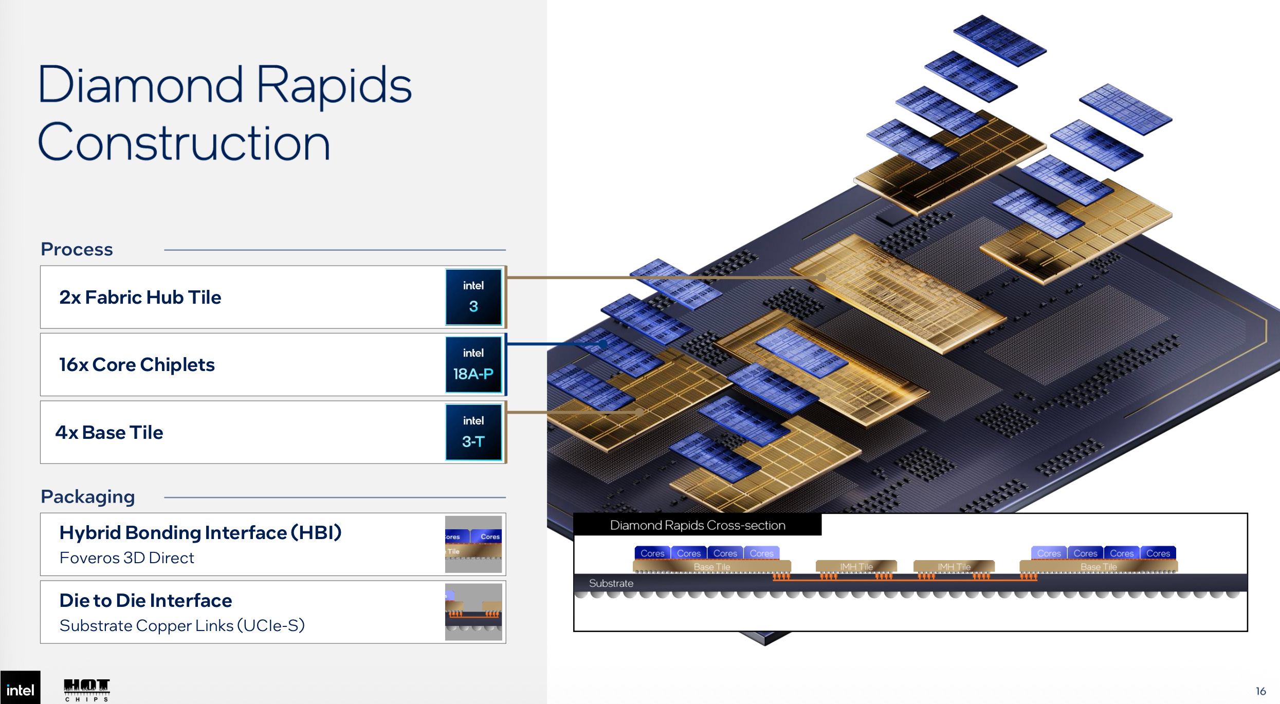
And then every part of the chip is Intel-made including the packaging. No TSMC.
NVIDIA Rubin GPU
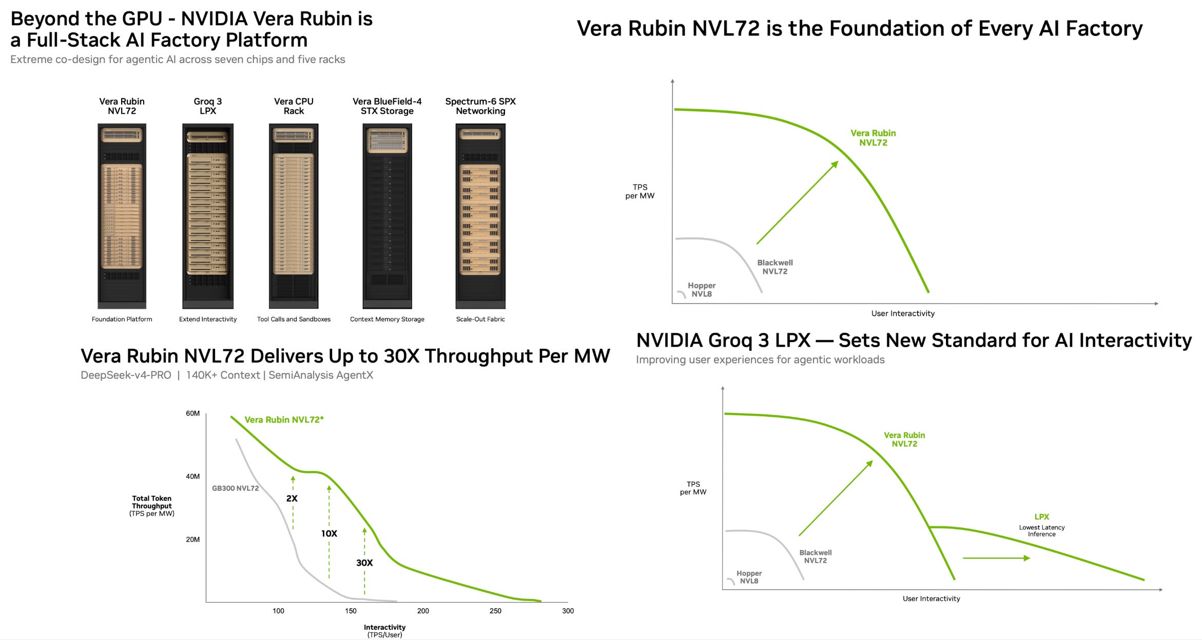
Hmmm the performance boost of Rubin over Blackwell is actually bigger on the high-interactivity (fast speeeeeed) side than the high-throughput one. 2x throughput in low interactivity while 30x throughput in high interactivity. We’ll see much faster tokens in a year.
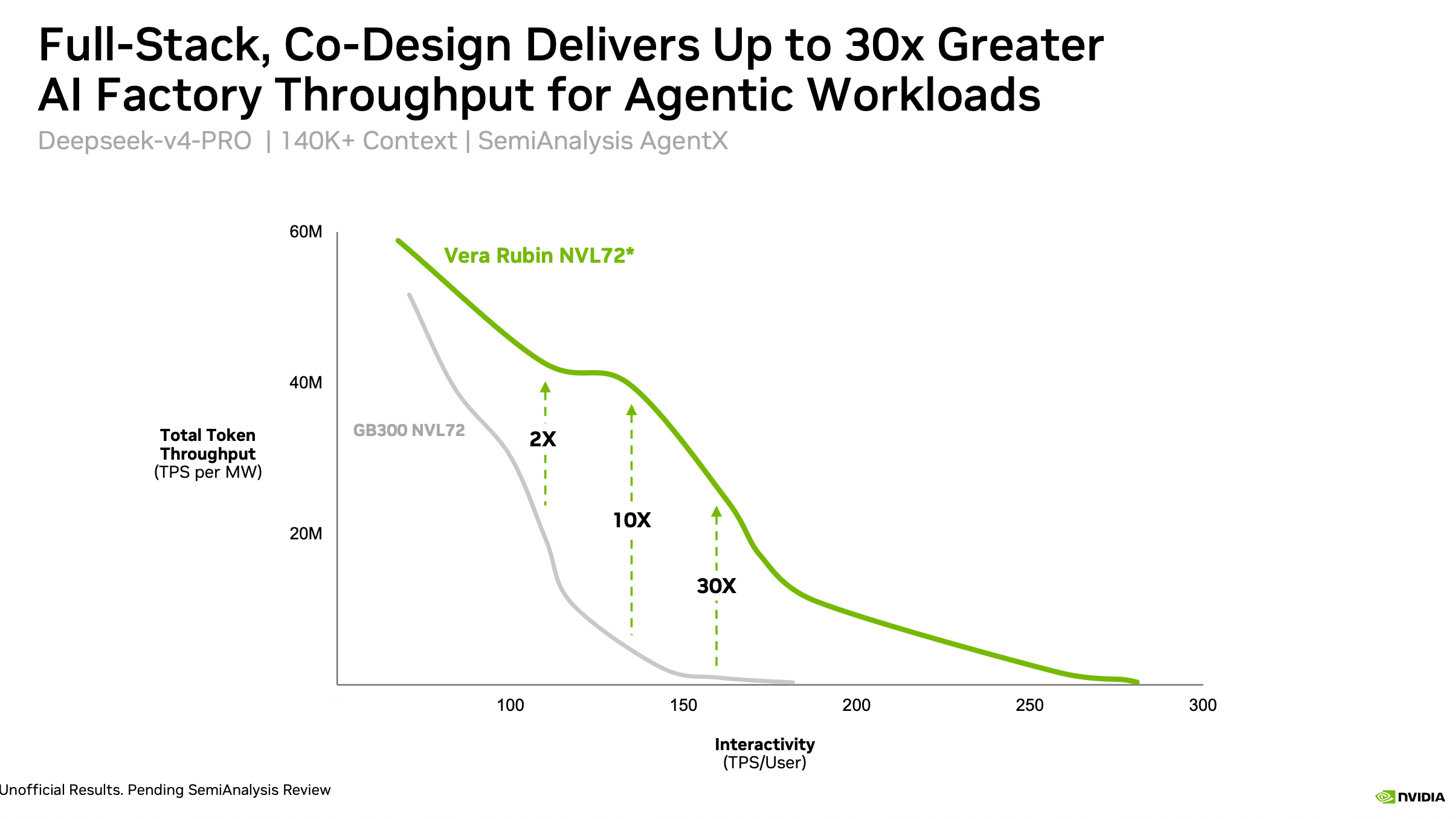
Likely because Groq LPX disaggs the decode and speeds it up. When you wanna go fast and you are bottlenecked by memory bandwidth you turn to super speedy SRAM.
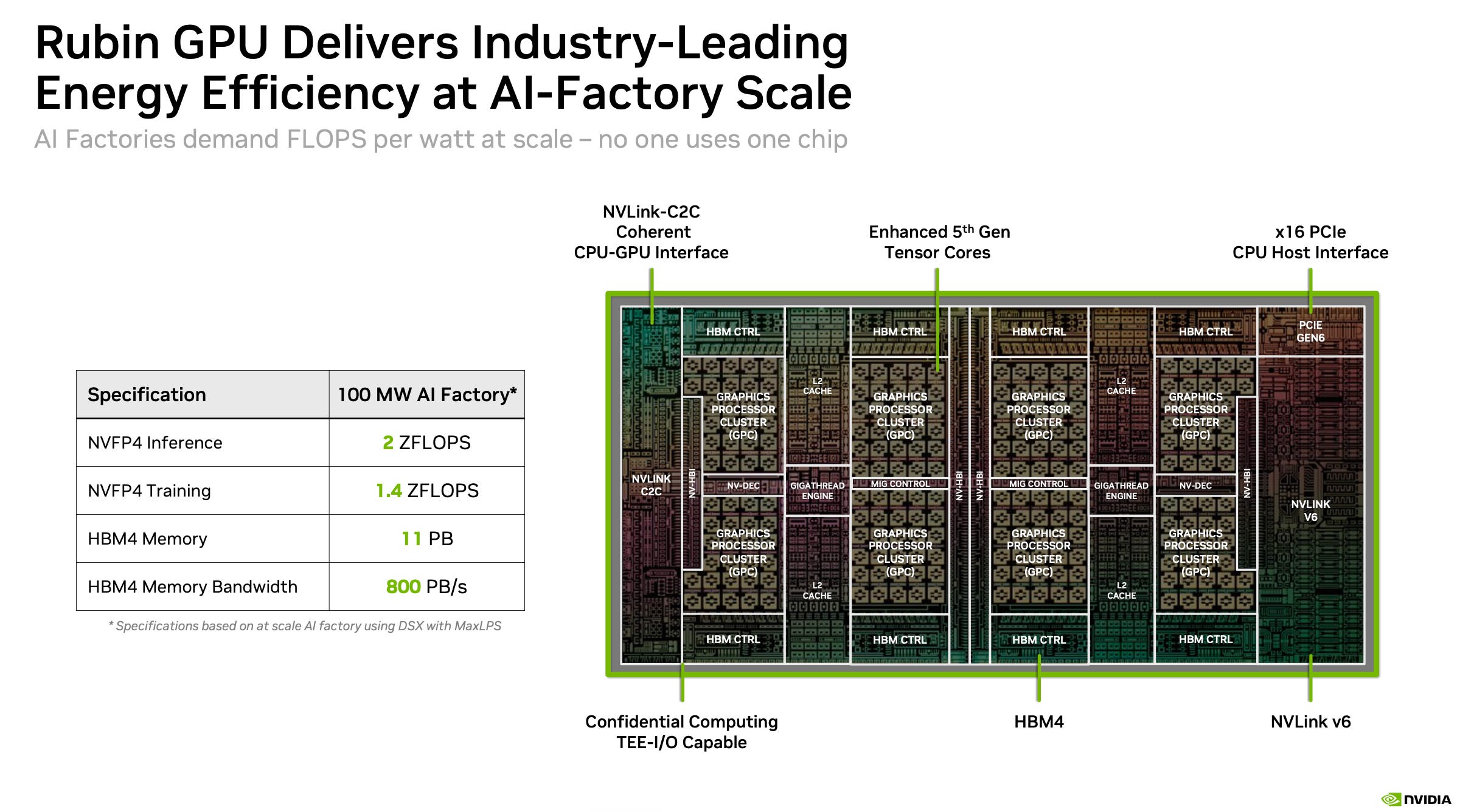
“No one uses a single chip”
It’s about the AI factory is a classic Nvidia-ism. High key I agree.
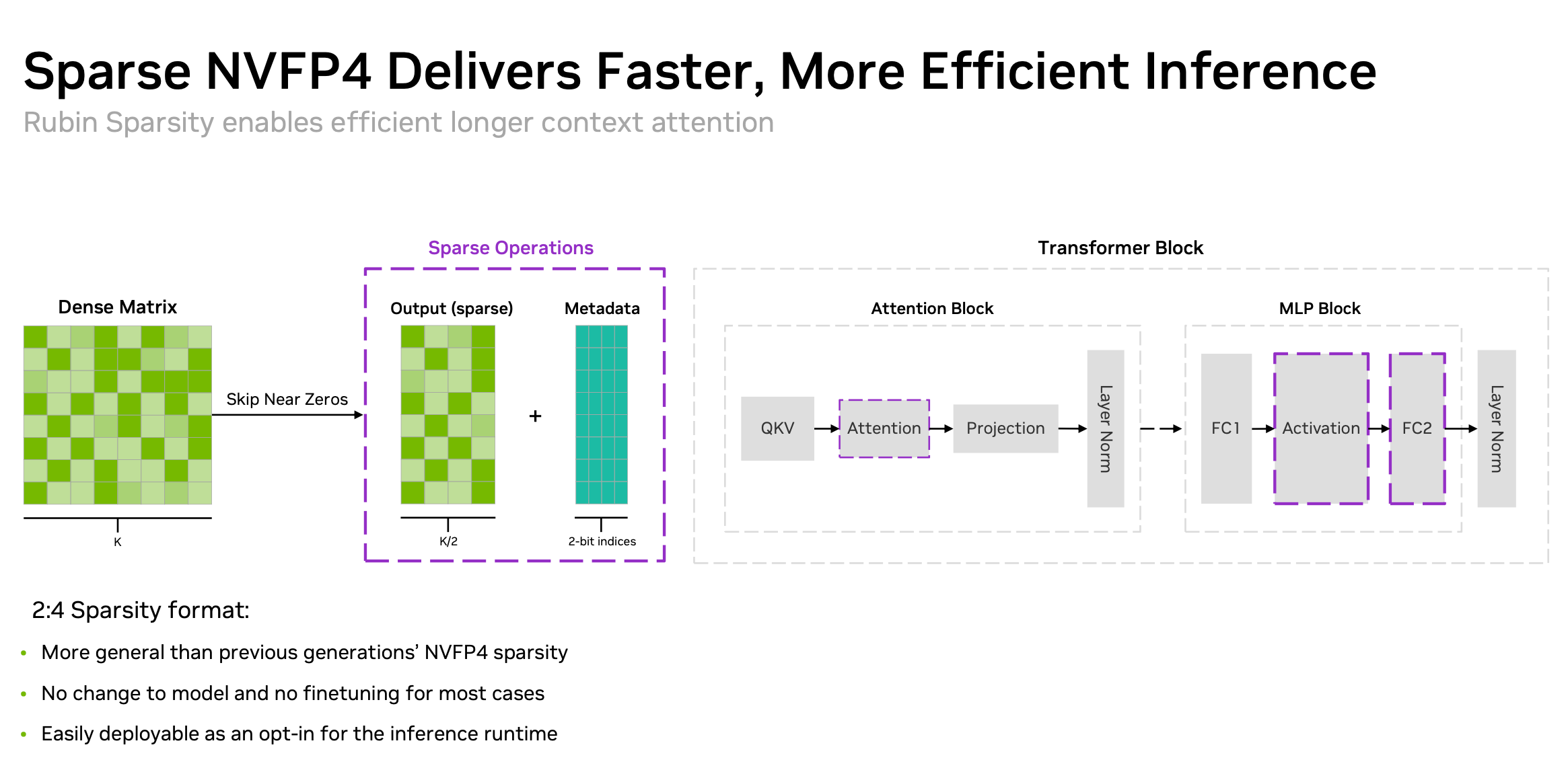
Rubin comes with adaptive sparsity. The relevant background is that quantization (whether your model weights are FP16 or 16-bit floating point numbers or like FP8 like how many significant digits your numbers have) is actually specific to the hardware and needs to be supported by the hardware. So they went from FP16 → FP8 → FP4 with Blackwell, but you can’t go to FP2 because you just can’t because you lobotomize the poor model.
So they invented adaptive sparsity. It’s basically taking the model and dropping the stuff that is near zero to make it half as big and replacing it with metadata.
NVFP4 here is actually a less quantized version of FP4. So it’s in between FP8 and FP4 and uses adaptive sparsity.
This is actually important because part of the software platform is specific to the hardware generation.
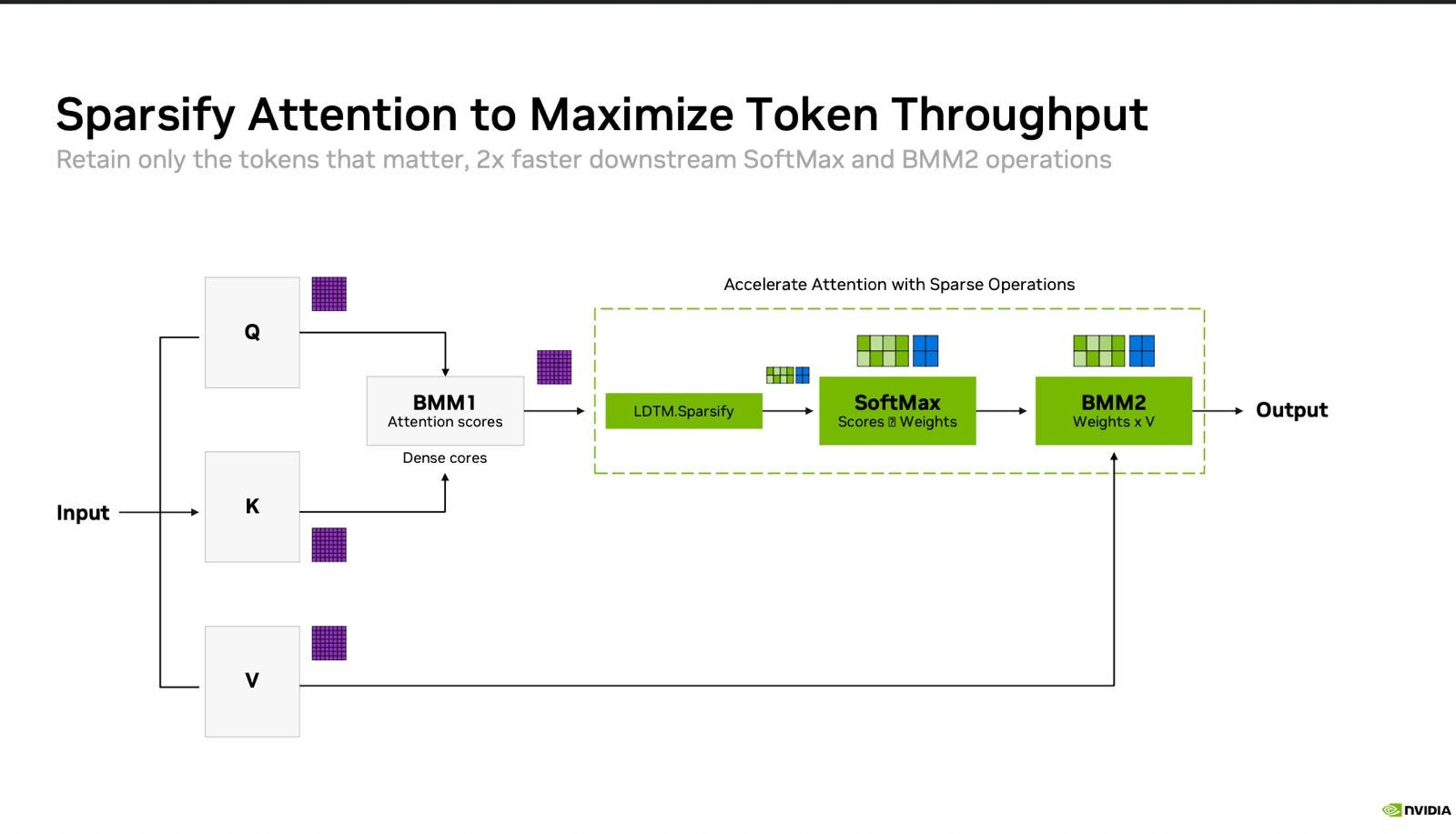
They also do sparse attention where you only do attention on tokens that matter instead of on every single token. Natively supported on Rubin. Basically taking a bunch of inference optimization software tricks and baking them into the hardware.
NVLink is a pretty important moat for Nvidia.
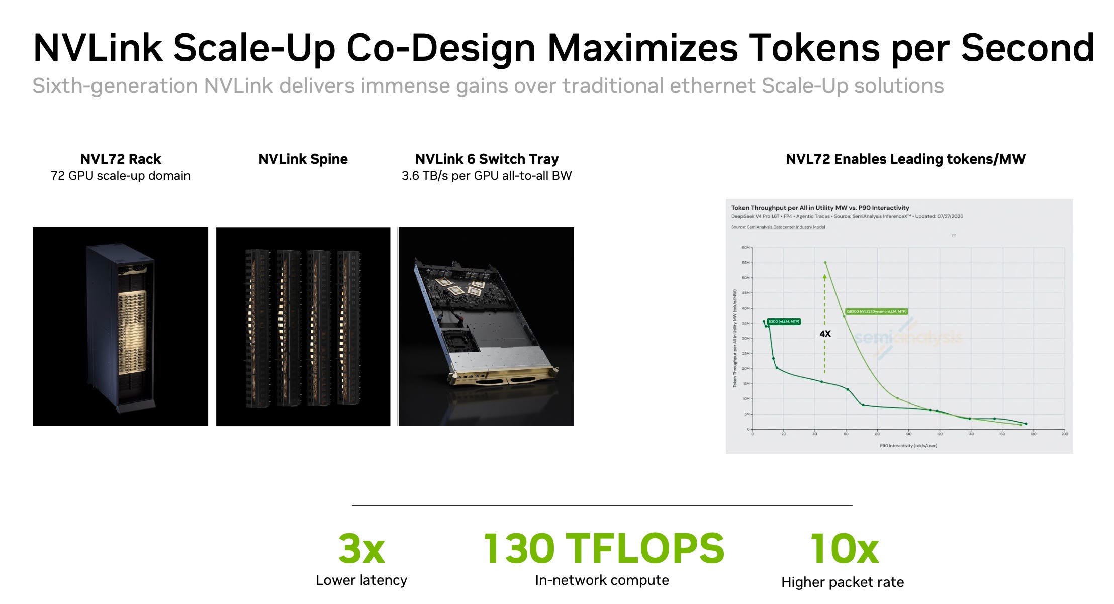
Large scale-up domains allow your racks to mog in the high throughput (cheap token) side of the curve. Via expert parallelism. Bigger scale-up domain means bigger batches. It’s the opposite of the Groq LPX.
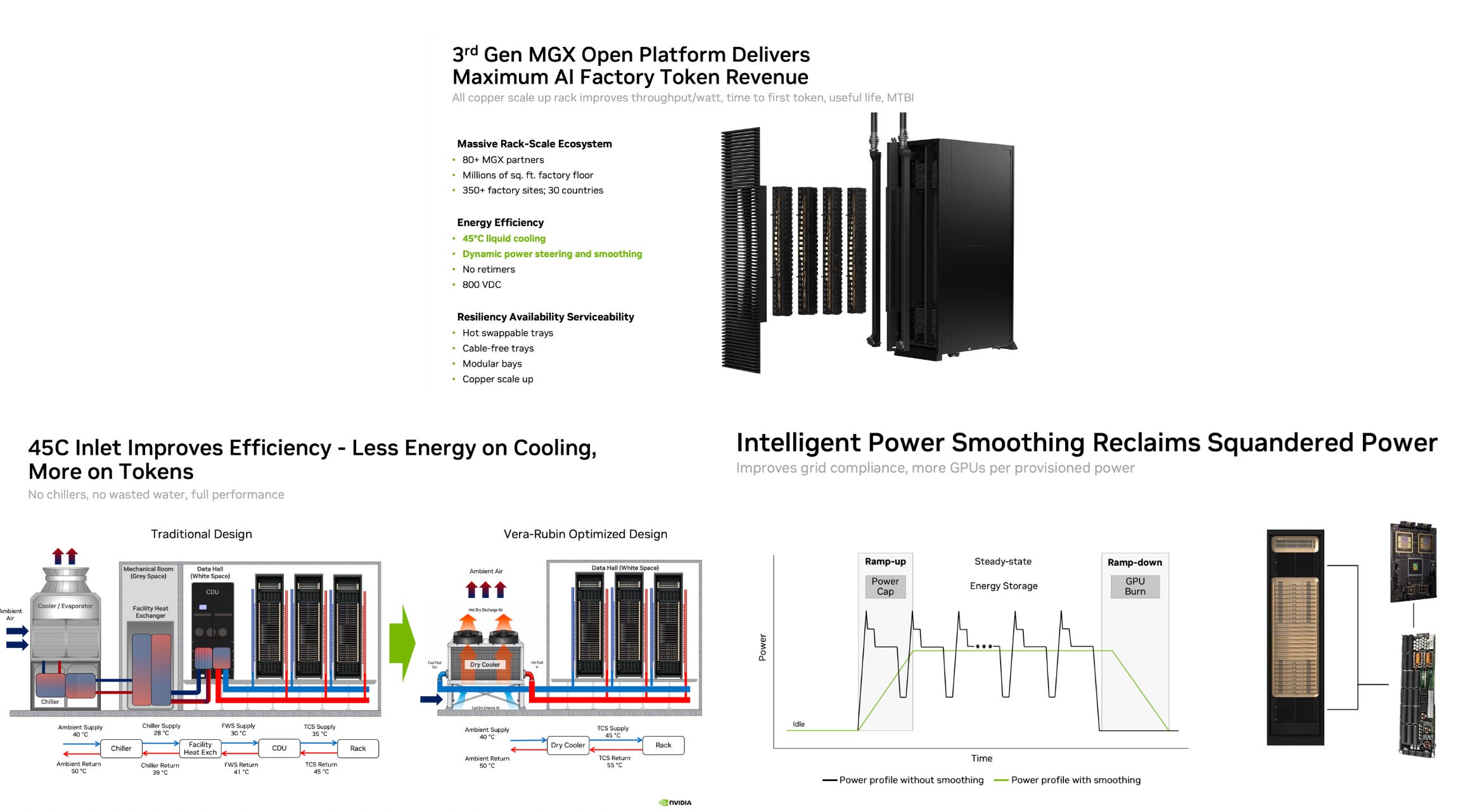
Some features of the rack: No optics (yet), 800VDC (sidecar), minimized cables, waste-less-stuff cooling, and smooth out your power with capacitors.
AMD Instinct MI400
AMD made a discount NVL72 that’s maybe not so discount.
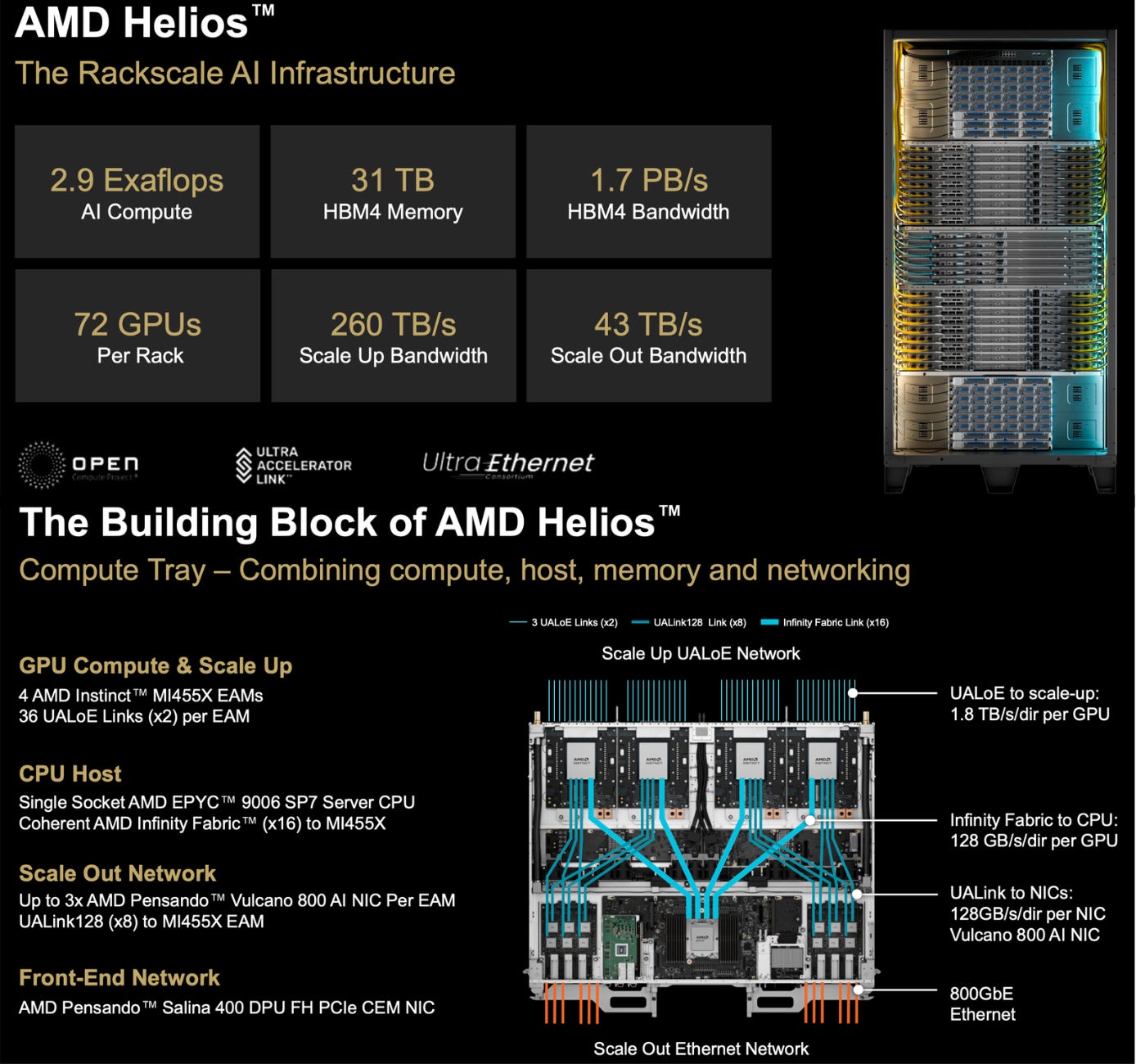
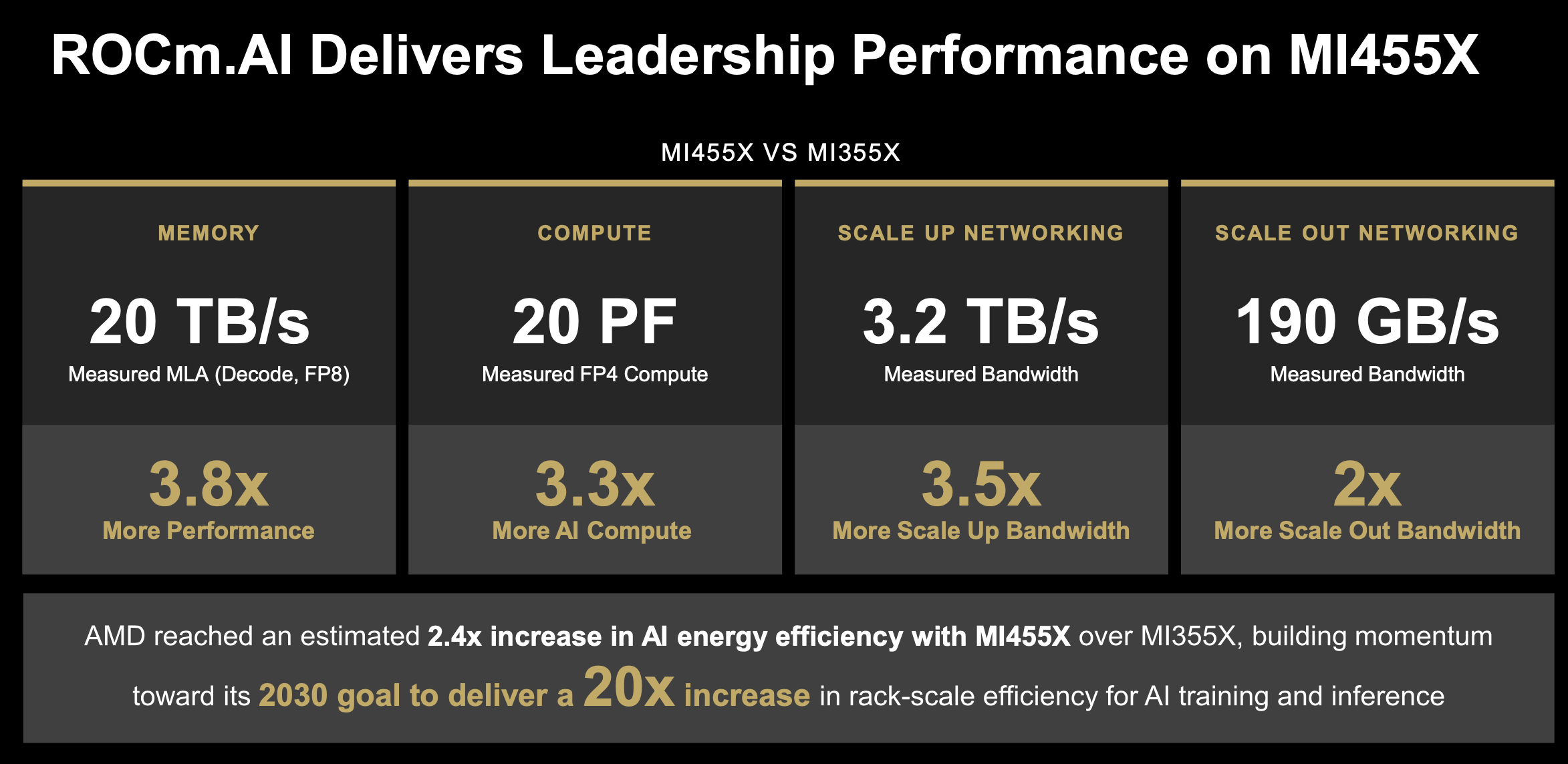
AMD’s rack actually beats or ties Nvidia VR200 NVL72 on pretty much all the specs. FP4 FLOPS and scale-up bandwidth are tied but AMD wins everything else.
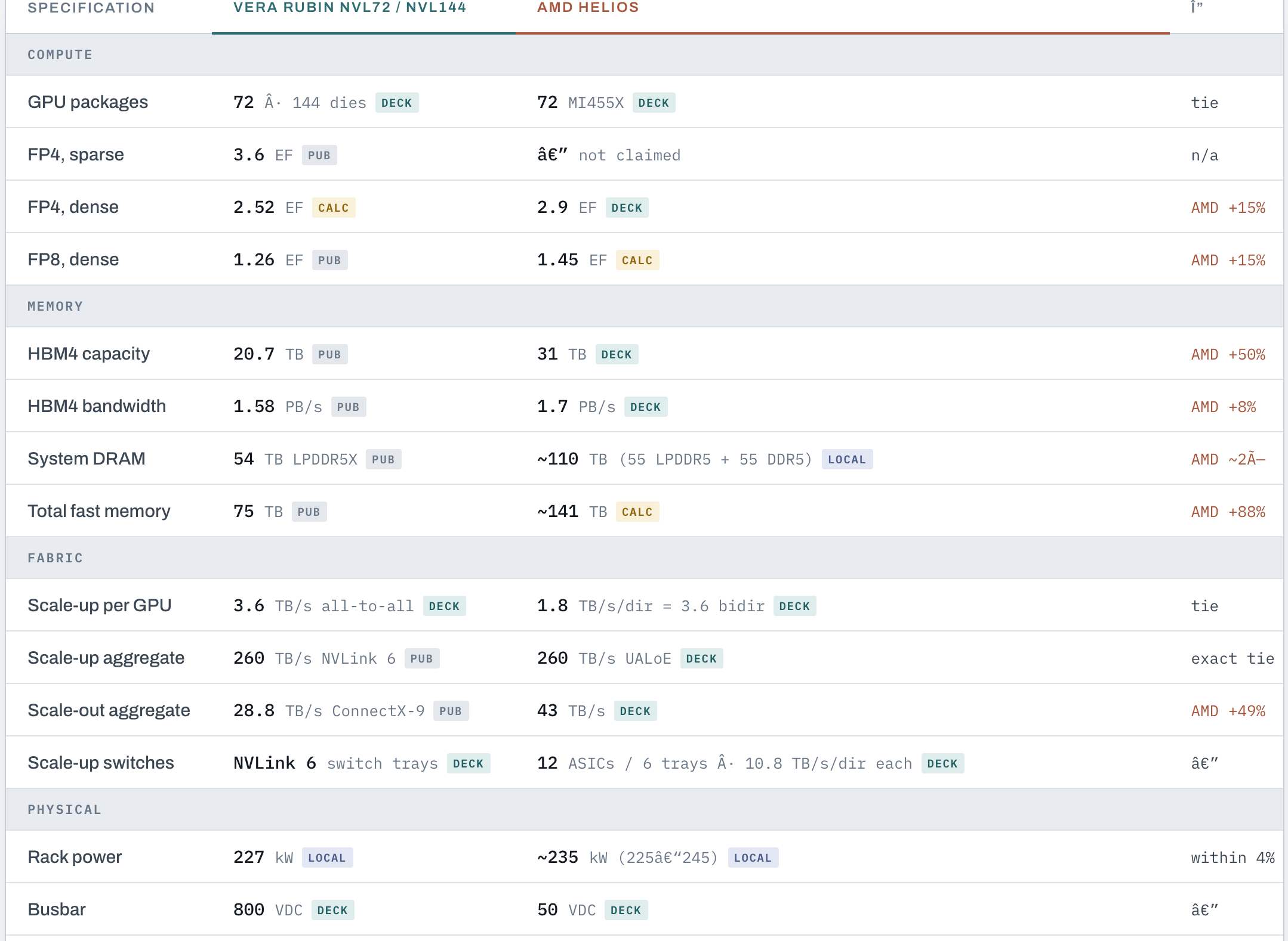
Especially memory capacity and scale-out bandwidth. The racks are almost the same power so technically you get denser per-MW performance. This is the AMD leapmog getting around whisper world.
What Nvidia has that AMD still doesn’t is NVLink. A good protocol co-designed with all your GPUs (and not open standard) is very important because when you do all-to-all the speed of the system is the speed of the slowest participant so you need to cut the tail.
And CUDA… but Nvidia doesn’t talk about that very much anymore. Wink wink.
Notice the key differences between the Nvidia and AMD presentations. Nvidia focused purely on system level performance type stuff while AMD’s slides are a giant spec sheet. It makes sense when you think about it. Nvidia, as the incumbent, has all of the models and software codesigned around it and thus can leverage its maturity to performancemaxx. The only way AMD could catch up is mogging in pure specs.
Next they did their system-level presentation. This is their scale-up pod architecture. Each one of these is one tray. 4 GPUs one EPYC connected to the scale-up switch.
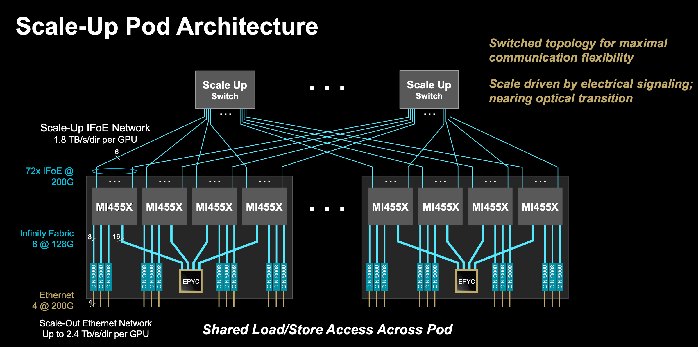
They said the next gen after this one will have optical. So same as Rubin Ultra.
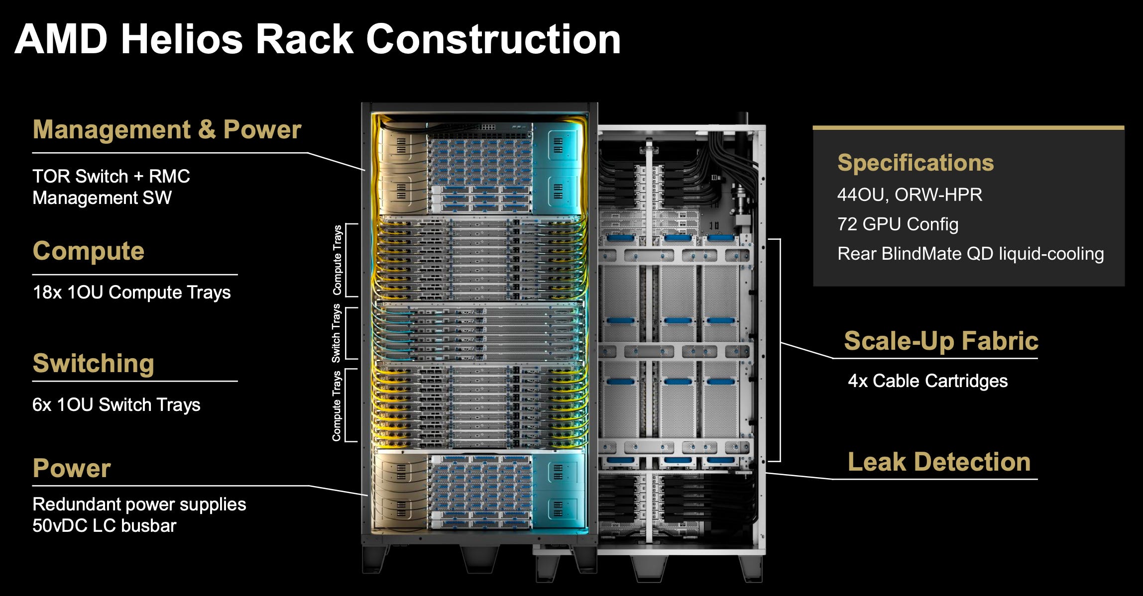
Not adopting 800VDC just yet. Also rack is kinda fat whereas Nvidia’s rack is skinny.
Intel Crescent Island GPU

This is Intel’s new attempt at datacenter GPU.
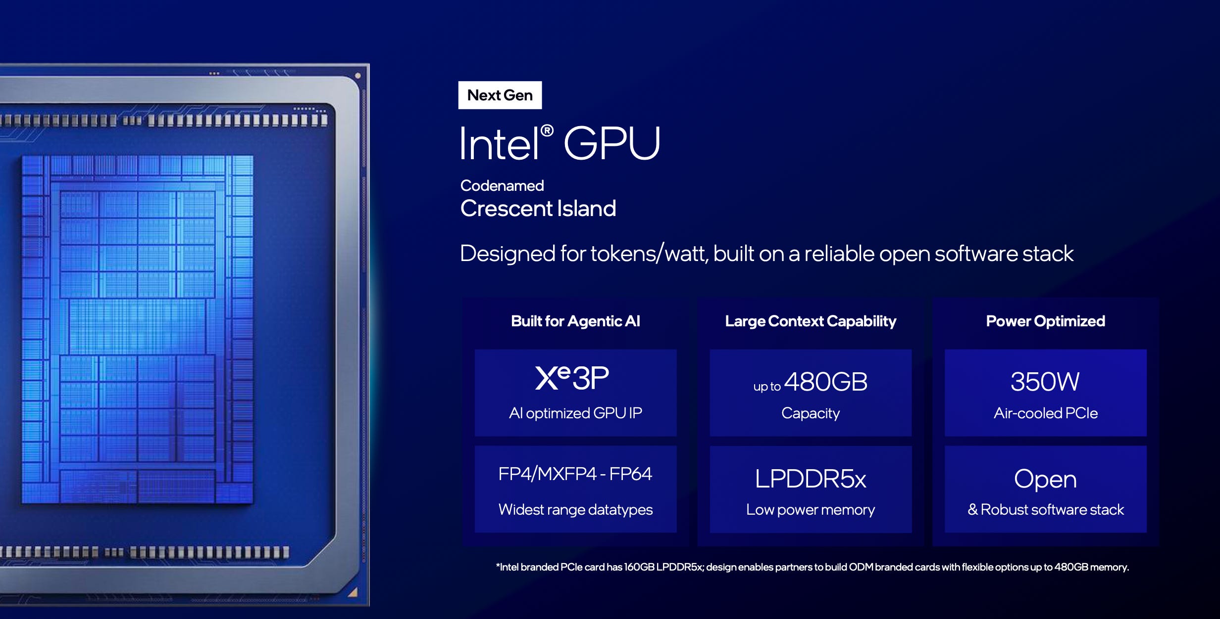
So it’s a no HBM, air-cooled, PCIe scale-up datacenter GPU! I am tryna think of who would use this but am coming up empty handed.
Intuitively it seems useful for not-latency-sensitive but very cost sensitive stuff. But for that you’d just want to go batch like crazy. And to do that you want big scale-up domain that you can’t get with PCIe scale-up.
Maybe for local/small enterprise private workloads?
Oh you know what I got it. If you just use this thing for prefill, you don’t need memory bandwidth. And then they have SambaNova’s SRAM widget for decode. Gonna be high interactivity expensive tokens only but could work? It also has 480GB of DRAM which is like double per-GPU HBM. Also it doesn’t need TSMC allocation because yk.
follow me on on X: x.com/jasonschips
Missed you man. Enjoyed reading!
Nice write up Jason! We must watch the infrastructure connecting and feeding the chips not just GPUs. Networking, memory bandwidth, scale-up interconnects, power, and system integration are becoming increasingly important bottlenecks.
But it's hard to tell who has the largest moat.