


Hot Chips is a based 3-day conference with a bunch of presenters and each day has its own distinct theme. Day 1 (today) is memory.
Very first thing you’ll hear about is how bad the memory shortage is lmao. It’s like 70% of a rack at this point and clearly the elephant in the room.
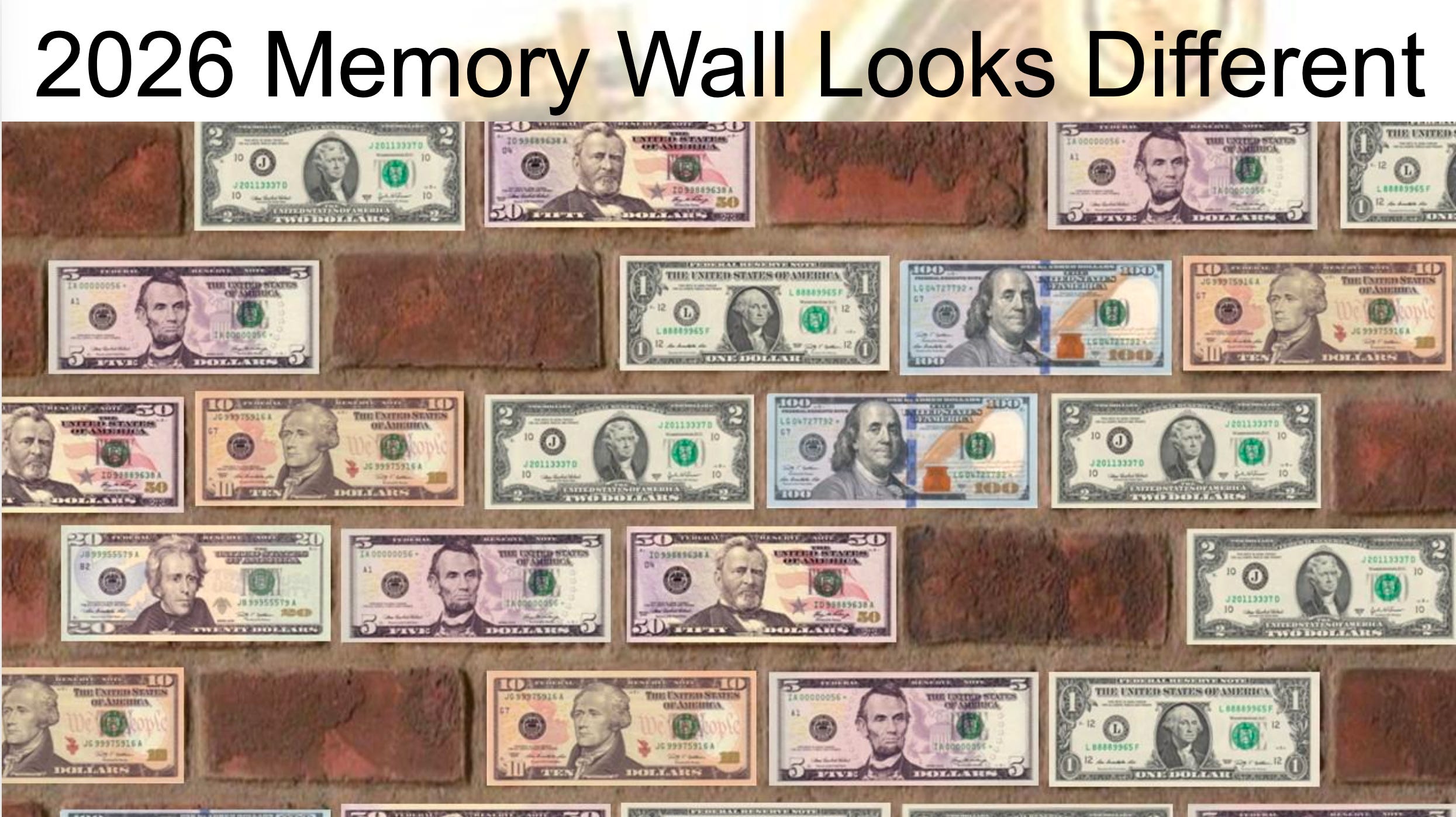
Not exactly the most bullish thing for DRAM makers if everyone at giant industry conference is dedicating their career to reducing price of your product.
For me and my conference coverage the idea is that I am not gonna immediately take a side and opine on whether or not something will work or will not work. I am investor not PhD. But what I will do is try to make these things as easy as humanly possible to understand via unfiltered brain dump.
Also, a funny theme to notice is that every company that presents just shills their own stuff. Like Samsung is gonna shill HBM-based die and processing in memory because guess who is the only memory maker with their own leading-edge foundry supply? SK hynix shills HBM because, well, they are SK hynix.
Contents
HBM Basics
Processing In Memory (Samsung)
HBM Packaging (SK hynix)
3D DRAM (d-Matrix)
High Bandwidth Flash (OXMIQ, PRAXMATI)
HBM Basics
Most of you know this but I always think it’s worth going over the fundamentals. High bandwidth memory has high bandwidth because it’s very parallel.
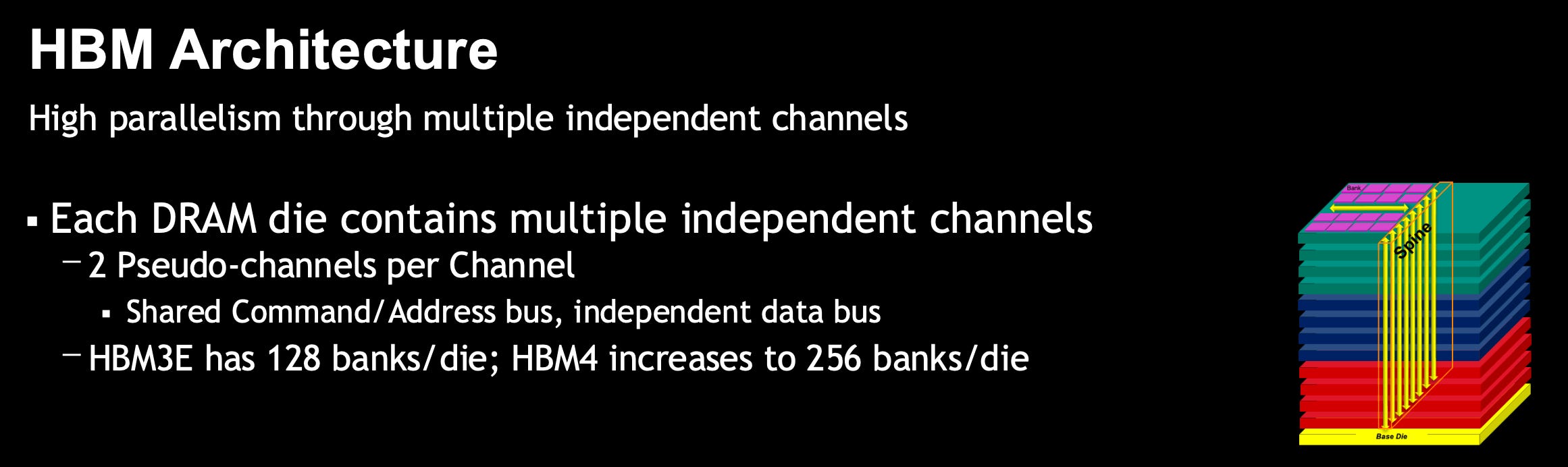
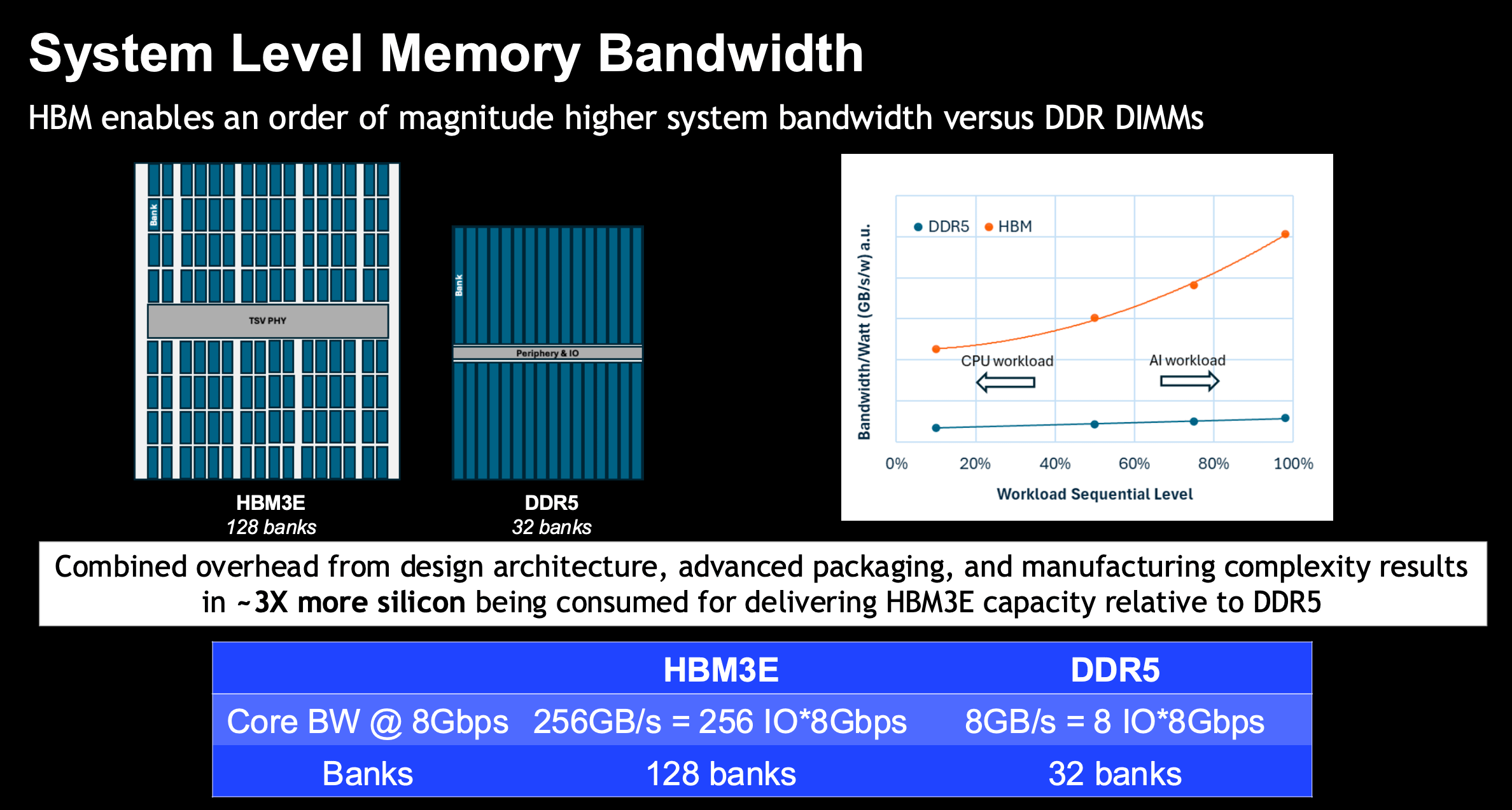
Therefore die needs to be bigger in order to allow this parallelism which contributes (but is not all of) to why HBM eats 3x die area vs DDR.
This conference (Hot Chips) was named after the main problem with HBM. which is that the chips get really hot.
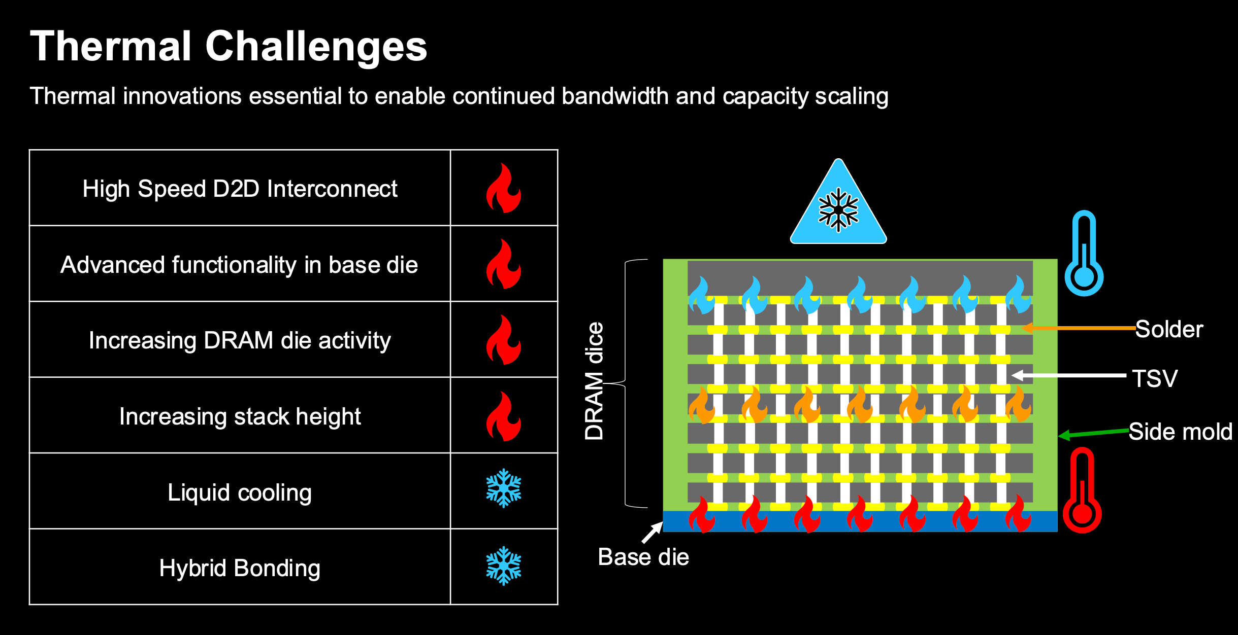
The problem is pretty intuitive actually. The cooling is on top not the bottom but the base die processor which creates the heat is all the way at the bottom therefore chip gets very hot. Reliability degrades at high heat.
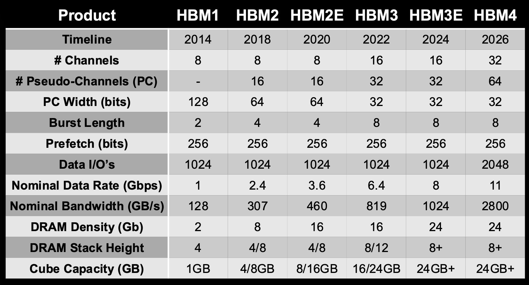
Some HBM stats:
Processing In Memory
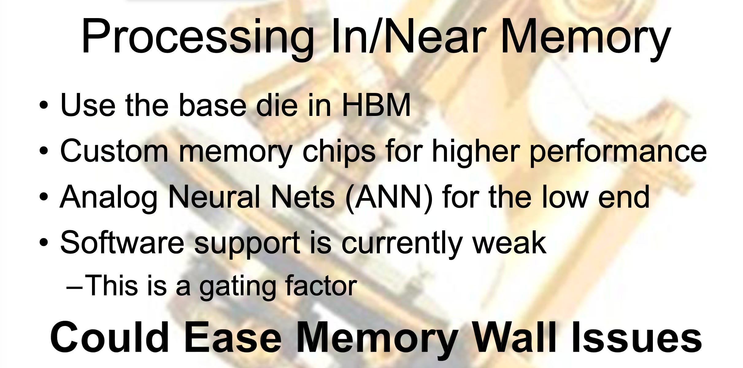
This is fascinating. General idea is that if you can do some computation on the base die, you have to send less data from HBM to logic die. Think about if you’re doing a complex math problem, instead of sending the entire starting problem back and forth between the memory and the processor, if the memory can get you to an intermediate solution already, you would only need to send that intermediate solution over to the processor. There is much less I/O.
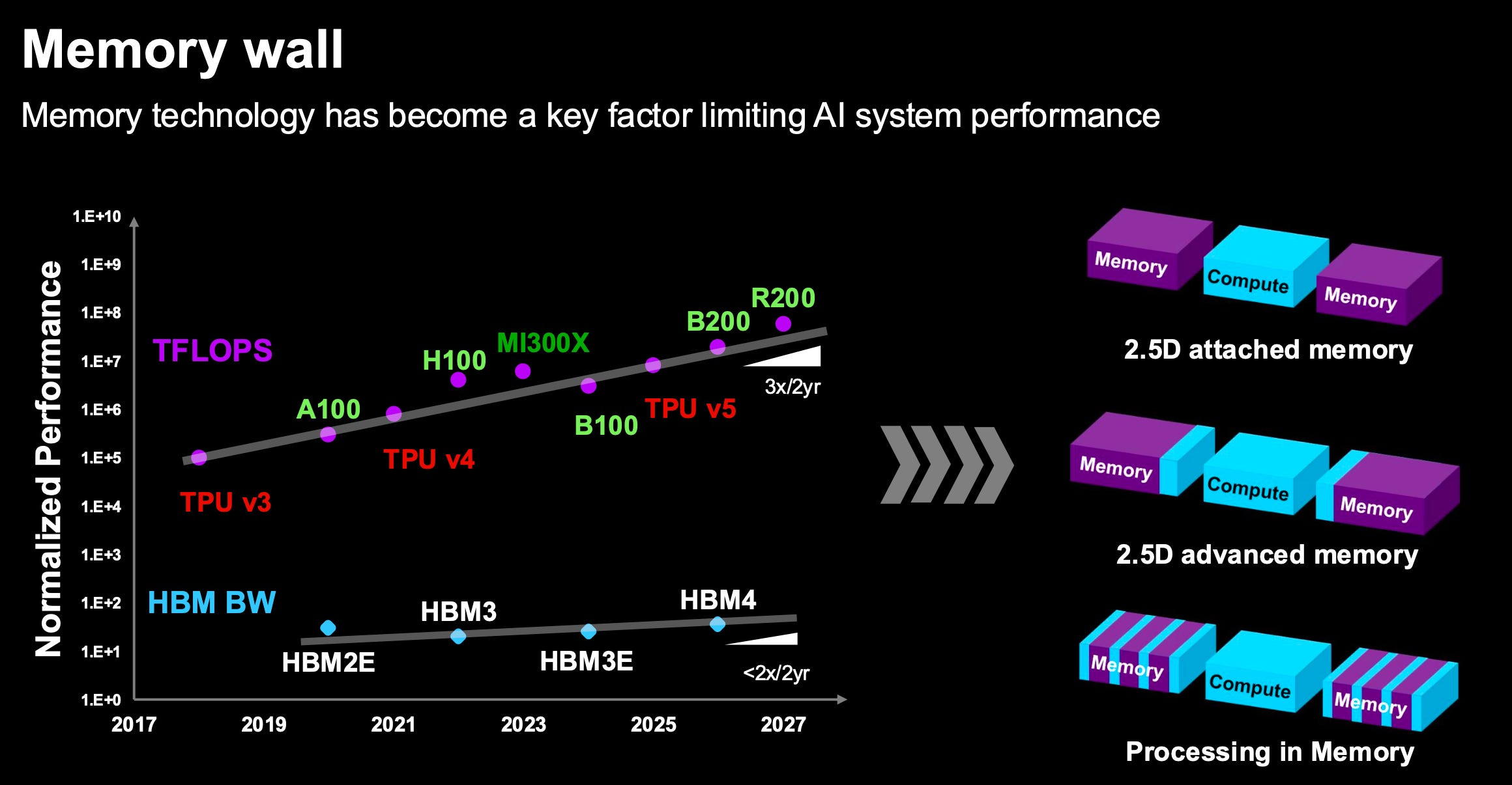
It is necessary because compute is scaling faster than HBM memory bandwidth. And decode (attention/FFN) is memory bandwidth bound so this is the exact thing you don’t want.
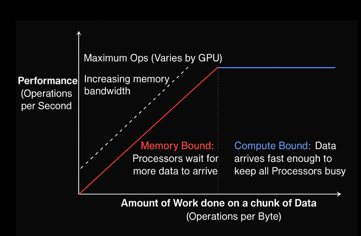
By reducing data transferred you also help the power requirement and therefore the thermals.

HBM base die currently is only a passive router, so arguably we can make it work harder. It only handles the communication channel to the compute die (the PHY) and test functions for the DRAM stack.
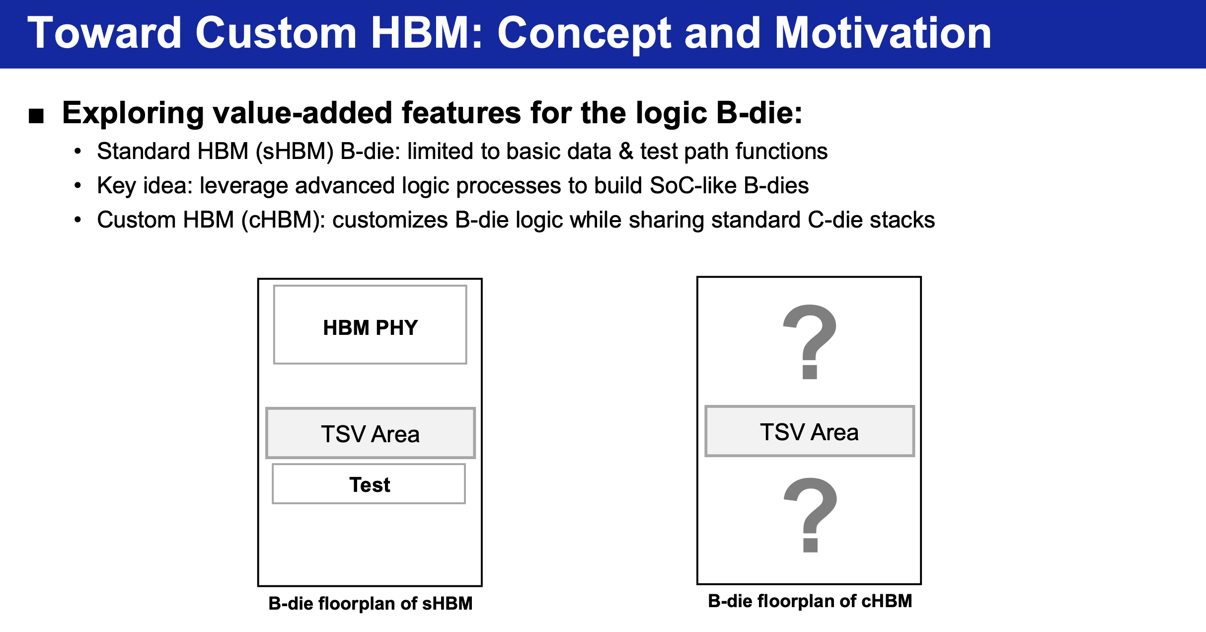
In the future base die can do a lot more stuff like the memory controller (moved off the xPU, freeing that area for compute), RAS sensors and self-test, connecting external memory directly through the base die, and eventually processing elements that do compute in the base die itself.
This also makes HBM a much more customized and less commoditized product.
This is obviously great for Samsung who has their own advanced logic foundry and doesn’t have to beg TSMC for allocation (like hynix and Micron) and also happens to make HBM. Also leading edge logic base die reduces power.

They can do this by reducing HBM PHY (portion of chip dedicated to the physical I/O interface that talks to the GPU) region. On advanced logic, the PHY shrinks to a small D2D interface. That frees up the rest of the die.
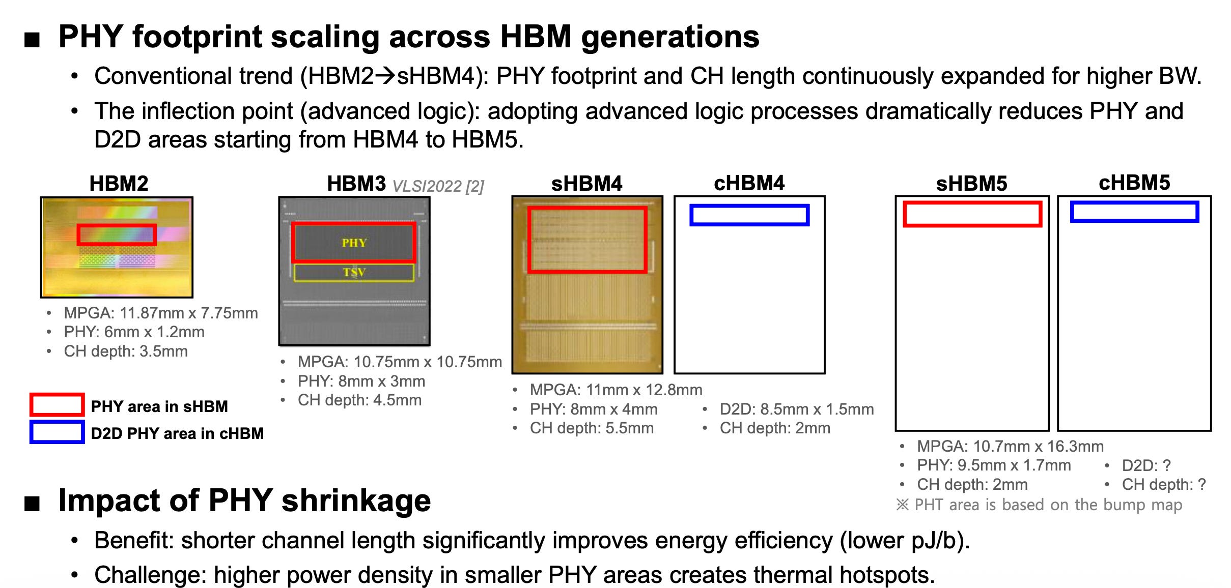
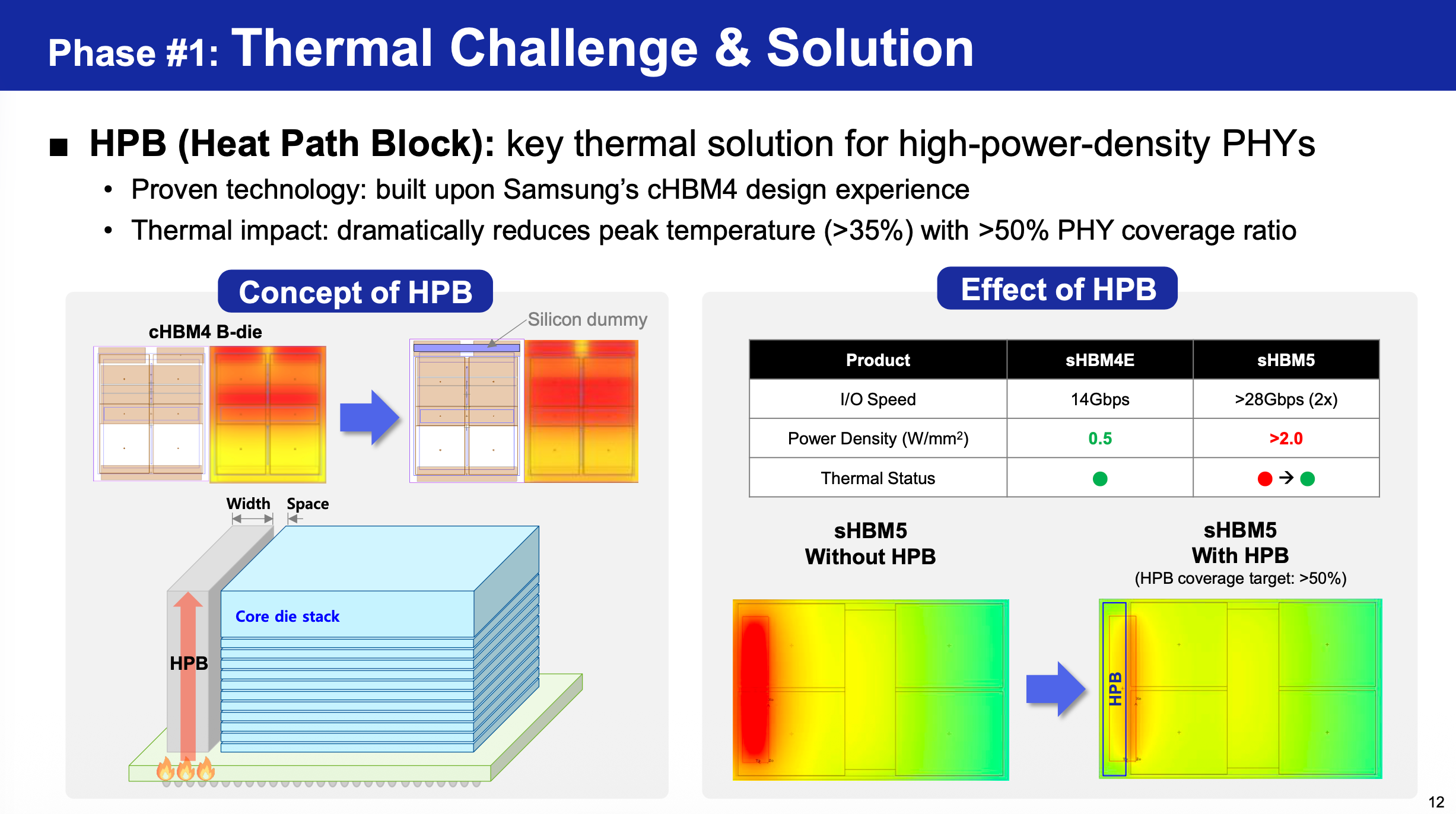
The challenge again is thermal hotspots due to higher power density.
And they actually have a pretty smart solution for this. PHY is hot. PHY is also on the side. So why not extract heat from side instead of top?
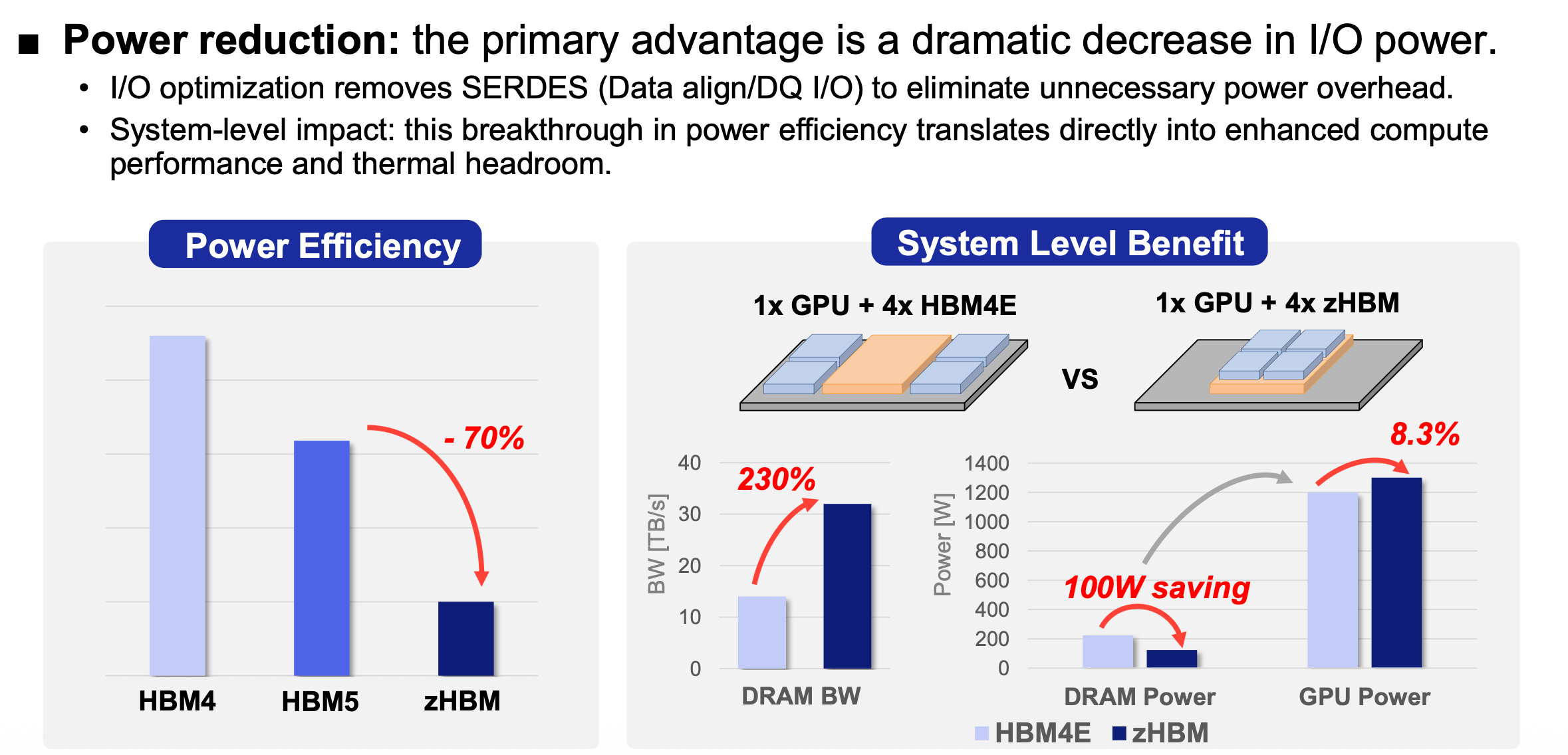
Next is zHBM. This is a common 2030+ type hype technology. Requires hybrid bonding and rocket science.
For ultimate bandwidth hack, just stack HBM on top of the XPU.
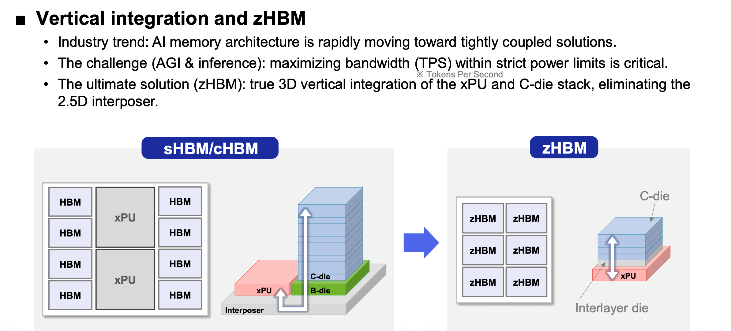
Can also reduce power significantly. Which is necessary to save thermals. Would also be 4 hi instead of 8 hi also in order to save thermals. So thermal issue might actually not be as big of issue.
Packaging
I still remember the days when MR-MUF was part of hynix moat thesis. SK hynix actually uses TC-NCF in HBM4 now.
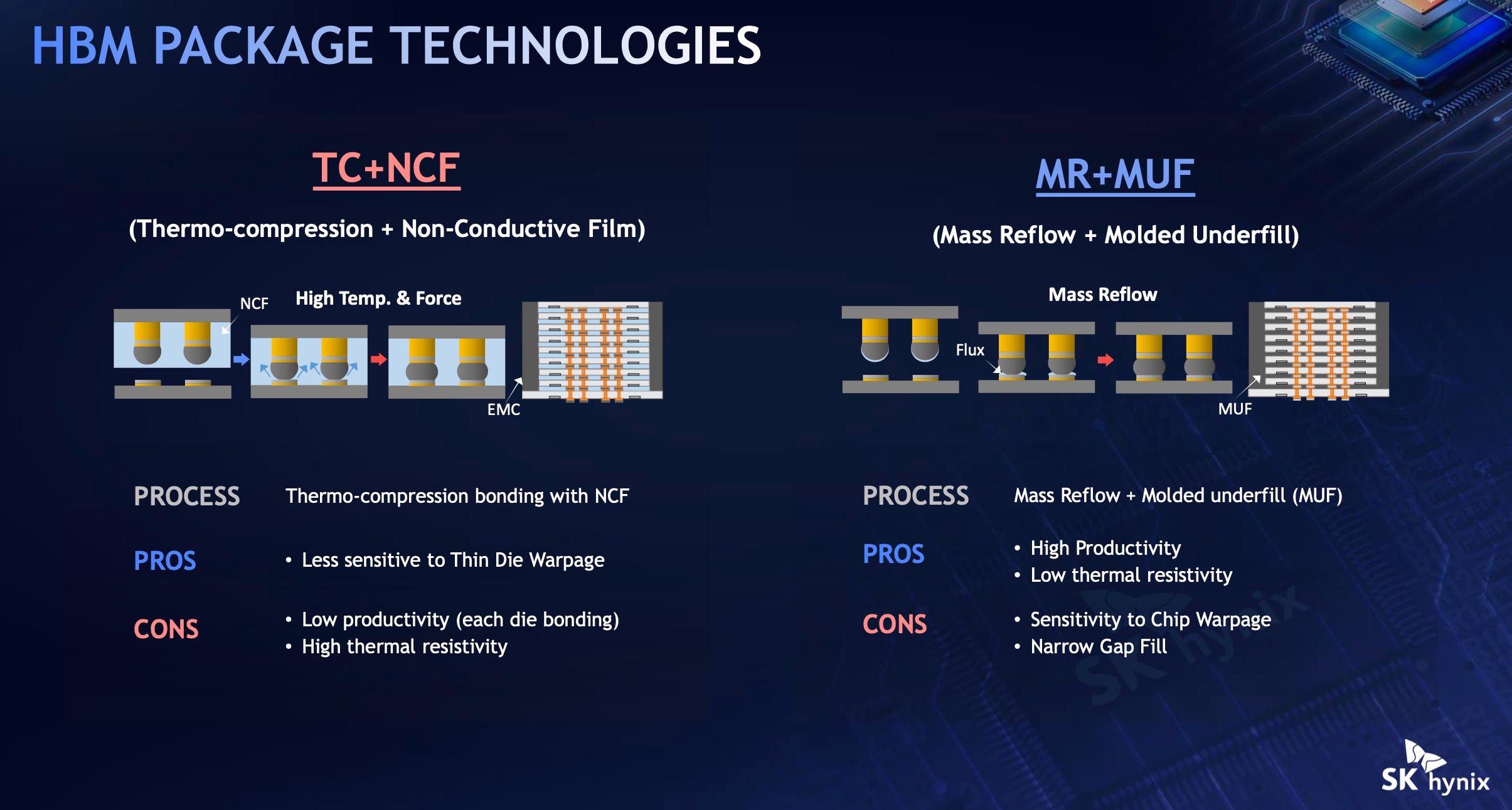
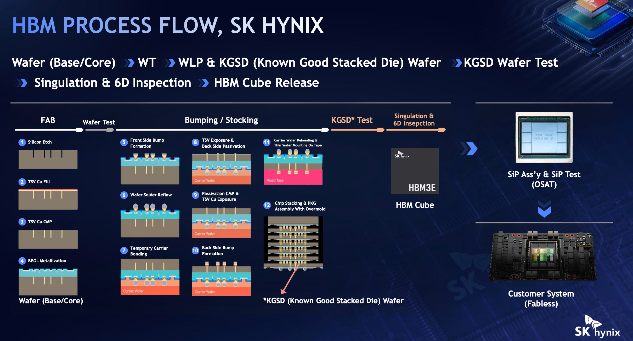
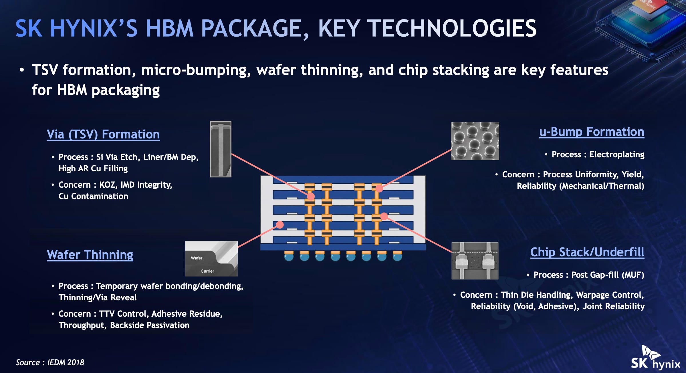
I don’t think there was anything too new about this presentation. This is the stuff that they’ve been doing since 2023 and doing a good job at.
3D DRAM
This presentation was objectively great. Very easy to follow and understand. Here goes my explanation.
SRAM is very fast but too big and expensive.
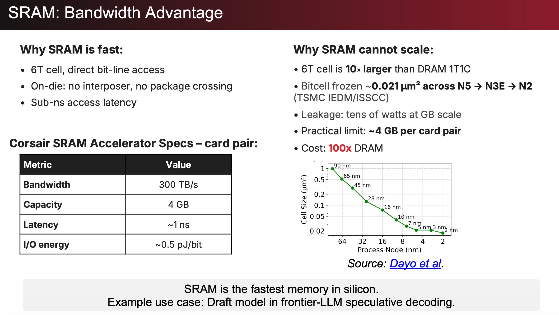
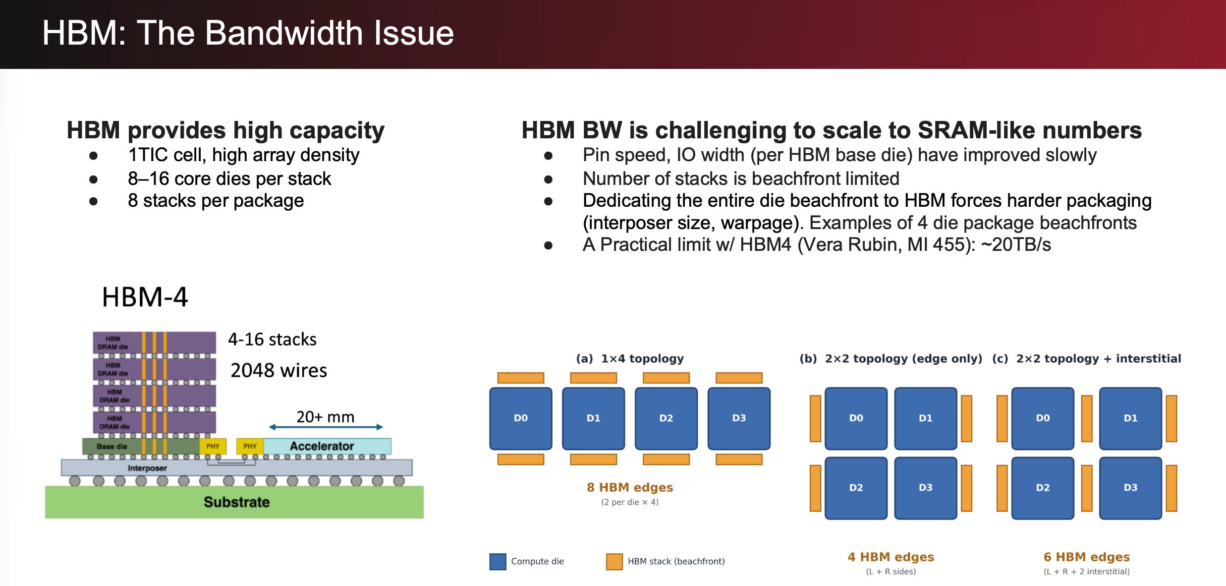
High Bandwidth Memory isn’t high bandwidth enough (but has great capacity).
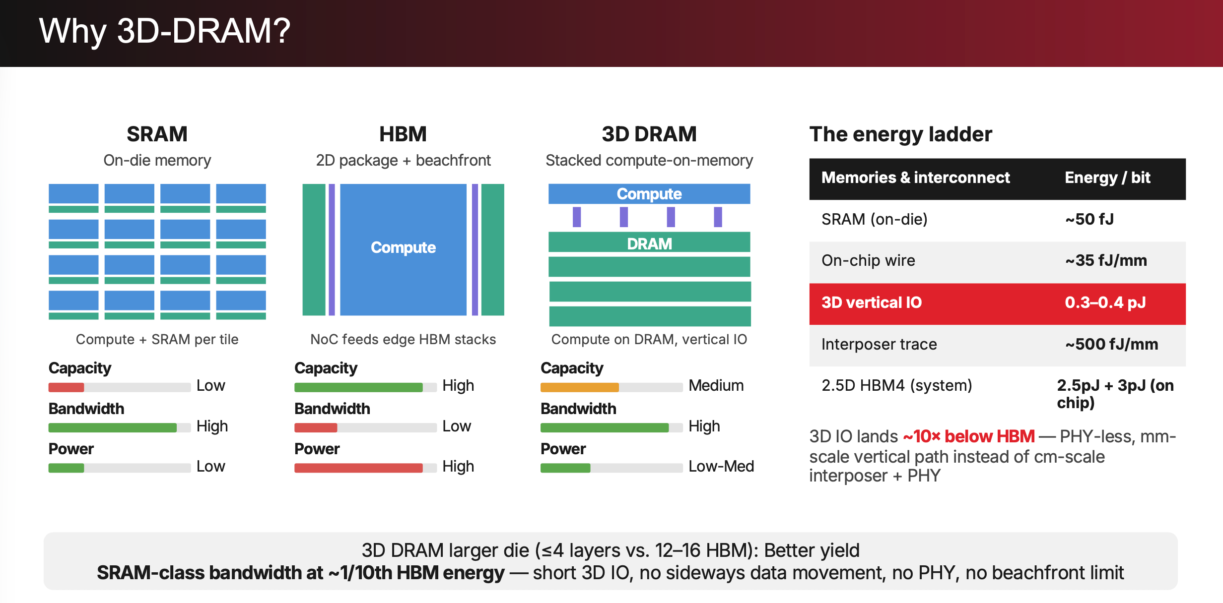
d-Matrix solution is stacking compute on memory which they call 3D DRAM. High bandwidth because no beachfront limitation and high capacity because it’s still DRAM.
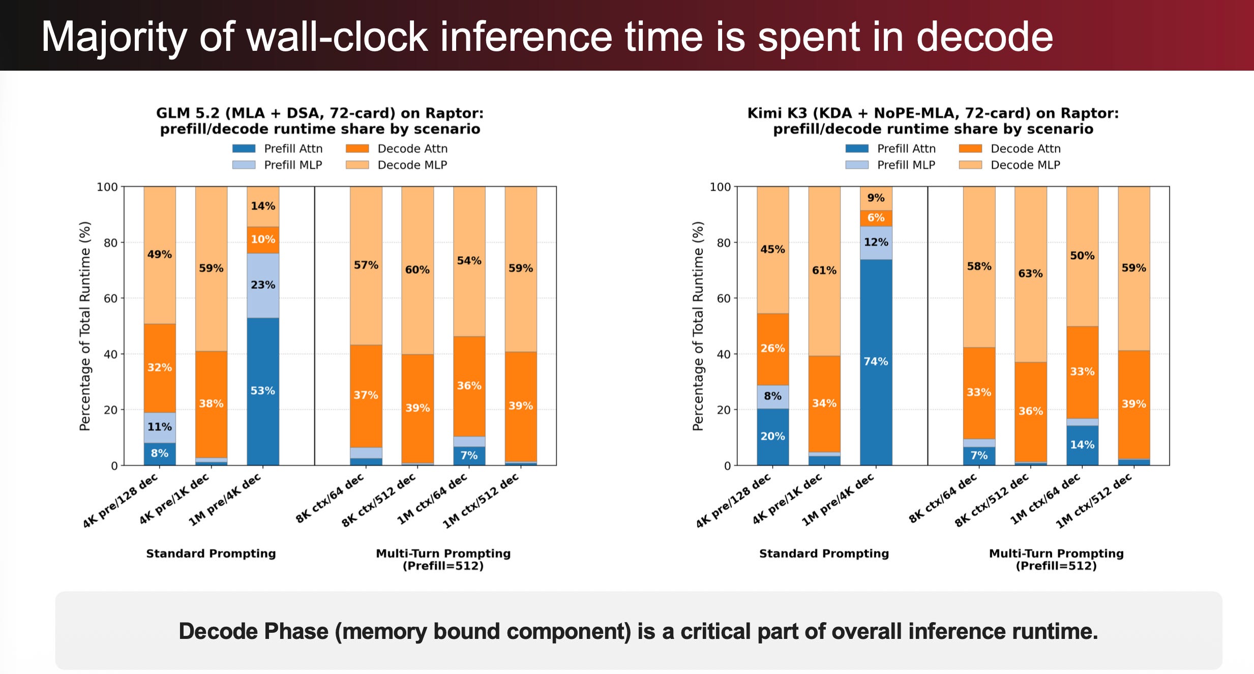
Most of inference time is spent on decode which is memory bandwidth bound.
Pitch is 3D DRAM = speedy inference that doesn’t bankrupt you.

This is actually really compelling. It’s not even funny. It’s like everyone’s breaking their neck trying these esoteric solutions, and these guys are literally saying to just stack logic on DRAM. It’s too simple: no multiple layers (it’s just one layer), no hybrid bonding. Just. Stack. The. Damn. Logic. On. DRAM.
High Bandwidth Flash
HBF is 8-16x the capacity of HBM.
But $/GB isn’t true TCO. What people actually care about is $/token. So you have to consider the tradeoff of bandwidth/latency which is 25x worse.
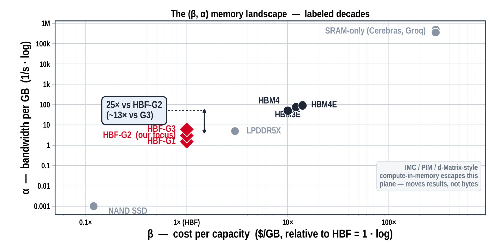
Memory bandwidth is important when you have high batch size (high throughput) and high interactivity (speedy inference). They are the opposite sides of the same tradeoff, so it is when you are pushing the Pareto frontier.
This graph is awful but maybe someone will find it helpful.
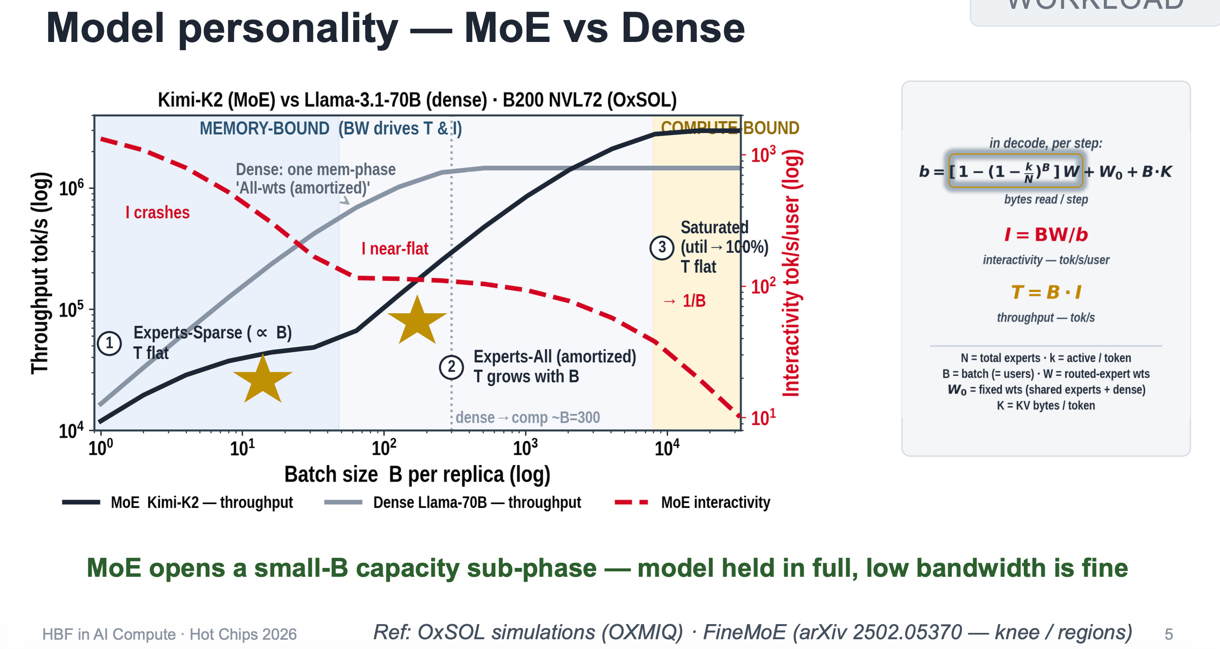
When you are trying to push that Pareto frontier you are memory bandwidth constrained and HBF will have tons of unused capacity.
HBF only useful for low batch size thus low bandwidth demand scenarios when you can use fewer GPUs & HBF stacks to serve the same tokens. So you can fill up the entire HBF.
Think about a small personal local or private enterprise workload. Smol box not big rack.
Another interesting use case is expert parallelism where in the FFN stage you put multiple experts on separate GPUs.
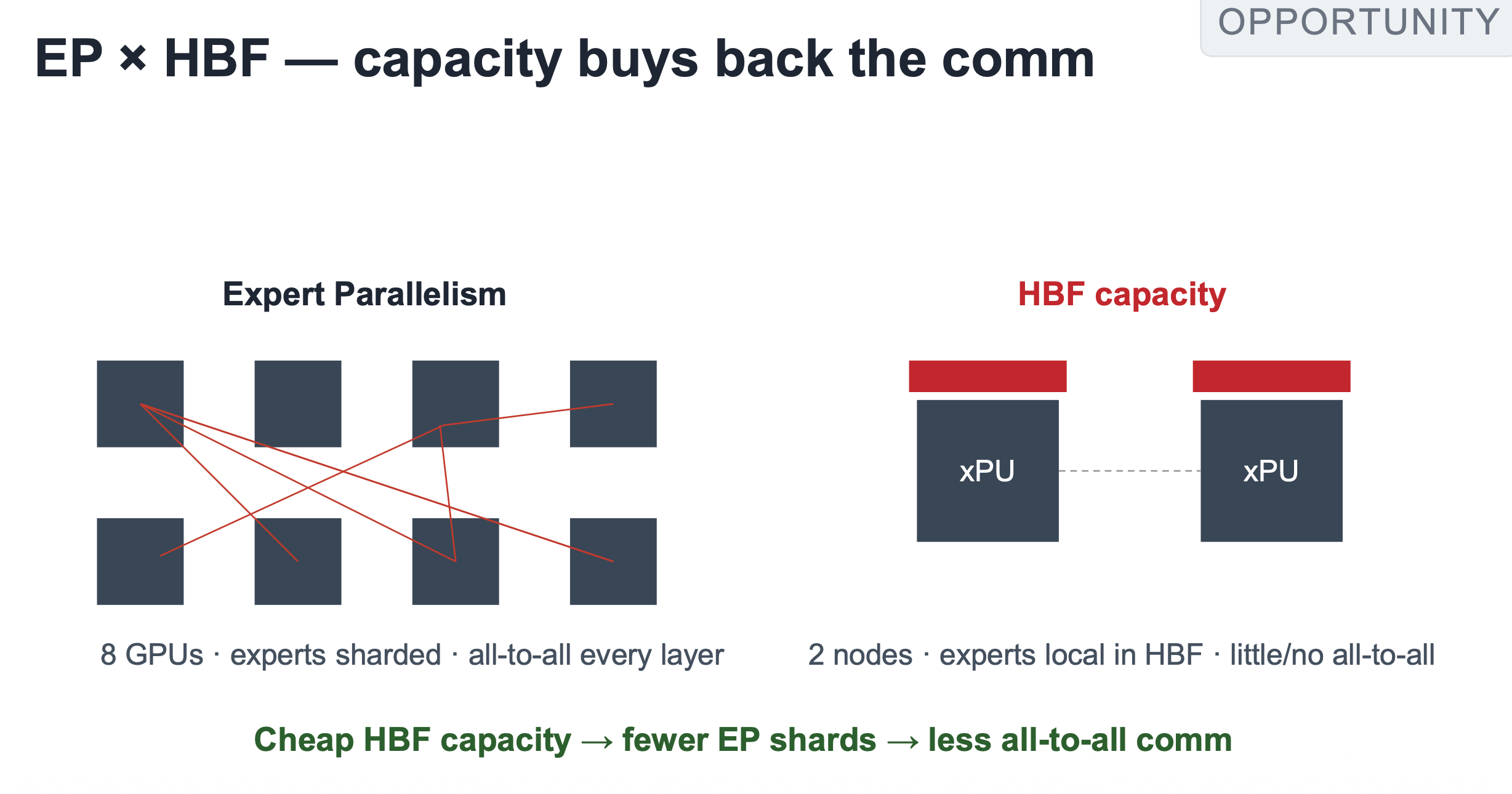
HBF thrives here because you cut down the amount of communication that is needed because more of the experts that are in the same place.
For HBF I was bullish going in but now am slightly less bullish and have more realism. If you haven’t seen Sandisk Investor Day they PUMPED. But it’s SanDisk. No, HBF does not have the same bandwidth as HBM. There is, in fact, a trade-off. But think about how mature the HBM ecosystem is and how much R&D has been poured into that, versus HBF. The fact that there are a few niche use cases today is kind of bullish because that means, as the software matures, as the systems get figured out, and as the actual design of the chip gets perfected, the HBM to HBF trade-off will start to go in HBF’s favor.
But if anything interesting does come up there NAND won’t even moon it will Mars. Think about it. HBM is like a 9x trade ratio because first you need SLC and not TLC and second you need to stack them like HBM.
Welcome back!! We missed you!! There is no other substack as good as yours 🙌🏻🙌🏻
This is the tell, right, if the industry itself is working to erase the shortage, the "shortage" story can't be the real reason for the price move. I wrote about the same pattern this week: same word explaining both the July crash and Friday's rally in memory names.