

Hot Chips is a 3-day conference held at Stanford where the industry’s chip architects present their newest designs, and it covers memory, CPUs, GPUs, networking, and custom accelerators from an electrical and computer engineeri

ng perspective. Each day has its own theme: day 1 was memory, day 2 was processing units, and day 3 was systems, networking, and custom silicon.
Why does a chip design conference matter to the market? It details the roadmaps of the most important companies in the space, which feeds directly into competitive positioning, especially in the fabless layer. One layer deeper, these roadmaps determine demand for specific hardware components, and this year that means memory above everything else. The memory shortage was the elephant in the room from the very first talk. Memory is now something like 70% of the cost of an AI rack, and you could feel every presenter designing around that number.
I have reorganized my 3 daily briefs into this full version, grouped theme by theme rather than day by day: memory first, then the CPUs, then the GPU racks, then the networking layer, and finally the custom silicon from the hyperscalers and startups. For each talk I give the gist of what was argued and the technical content that backs it, and I draw the implications together at the end of each theme. At the end I pull the whole conference into the takeaways.
Contents
Memory
CPUs
GPUs
Networking
ASICs
Conference Takeaways
Memory
The memory day opened with a tutorial and then turned into 6 different companies presenting 6 different ways to attack the same problem. The problem is that AI compute keeps scaling roughly 3x every 2 years while HBM bandwidth scales less than 2x, so the gap between how fast a GPU can do math and how fast memory can feed it keeps widening. Every talk on the memory day is a different answer to that gap, and they all share 1 move, which is putting compute closer to where the data lives.
HBM Basics
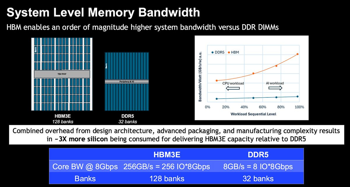
High bandwidth memory has high bandwidth because it is very parallel. A regular DDR5 module talks to the CPU over a 64-bit bus, while an HBM stack talks to the GPU over 1,024 wires (2,048 on HBM4), all running at roughly the same per-wire speed. The entire bandwidth advantage is width, and the width comes from stacking DRAM dies on top of each other and punching thousands of vertical connections, called through-silicon vias (TSVs), straight down through the stack into a base die that talks to the GPU.
That parallelism has a cost. The die needs to be bigger in order to allow all those connections, which is part (but not all) of why HBM eats roughly 3x the die area of DDR for the same bits. Micron’s presenter put a number on it: the combined overhead from the architecture, the advanced packaging, and the manufacturing complexity consumes about 3x more silicon per bit of HBM3E capacity relative to DDR5. Every wafer of HBM is a wafer of regular DRAM that never got made, which is a big part of the shortage.
Provide a caption (optional)
The second cost is heat. The cooling sits on top of the stack, but the base die that creates most of the heat sits all the way at the bottom, so heat has to travel up through 8-16 layers of DRAM before it reaches the cold plate. DRAM hates heat, since hot cells leak charge faster and need more frequent refresh, so reliability degrades exactly where the architecture concentrates the heat.
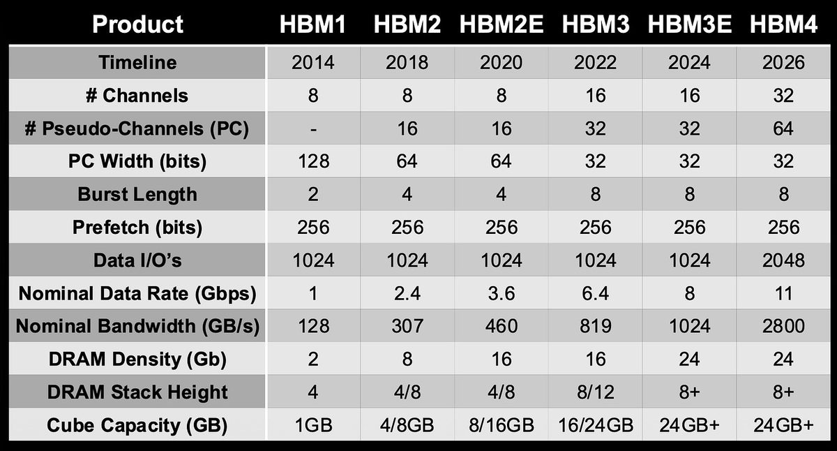
HBM specs over time:
Provide a caption (optional)
Samsung Custom HBM
Samsung’s talk argued that the HBM base die should become a computing element rather than a passive router, and that argument conveniently requires a leading-edge logic foundry, which Samsung happens to own. The general idea of processing in memory: if you can do some computation on the base die, you have to send less data from HBM to the logic die. In a complex math problem, instead of sending the entire starting problem back and forth between the memory and the processor, if the memory can get you to an intermediate solution already, you only need to send that intermediate solution over, so there is much less I/O.
This is necessary because compute is scaling faster than HBM bandwidth. Inference runs in 2 phases: prefill, where the model reads your whole prompt, and decode, where it generates tokens 1 at a time. Decode is memory bandwidth bound, because generating each token means re-reading the model’s weights and the conversation’s working memory (the KV cache) from HBM, so the widening gap lands on exactly the phase where the money is. By reducing data transferred you also help the power requirement and therefore the thermals, since moving bits burns most of the energy in the first place.
The HBM base die today is only a passive router, and Samsung’s pitch is that it can work harder. It currently handles the communication channel to the compute die (the PHY) and test functions for the DRAM stack. Samsung’s roadmap runs in 3 phases. Phase 1 moves the base die from a DRAM process to 4nm logic starting with HBM4, shrinks the PHY (the portion of the die dedicated to the physical I/O interface that talks to the GPU) into a small die-to-die interface, and offloads the memory controller from the GPU, freeing GPU area for compute. Phase 2 adds functions to the freed-up space: RAS sensors and self-test, connections to external memory routed directly through the base die, and eventually processing elements that do compute in the base die itself. Phase 3 is full 3D integration.
This also makes HBM a much more customized and less commoditized product, which is the strategic point inside the engineering talk. This is great for Samsung, who has their own advanced logic foundry and does not have to beg TSMC for allocation (like hynix and Micron do), and also happens to make HBM. A leading-edge logic base die reduces power too.
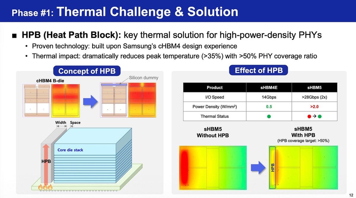
The challenge again is thermal hotspots from the higher power density of logic on the base die. And they actually have a pretty smart solution. The PHY is hot. The PHY also sits on the side of the die. So why not extract heat from the side instead of the top? They showed a heat-path block (they call it HPB) running up the side of the stack, targeting more than 50% coverage, and their simulations show it pulling the sHBM5 thermal picture from red back to green.
Provide a caption (optional)
Next is zHBM, the 2030+ step on this roadmap. It requires hybrid bonding (fusing dies together copper to copper, no solder bumps). For the ultimate bandwidth step, you stack the HBM directly on top of the GPU, eliminating the interposer (the slice of silicon the GPU and HBM currently sit on side by side) entirely. The claimed numbers are large: 70% lower power versus HBM5, 230% more DRAM bandwidth at the system level, and a 100W saving per GPU package. It would also run 4-high instead of 8-high to save thermals, so the thermal issue might be smaller than it looks.
SK hynix HBM Packaging
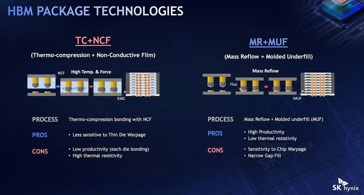
I still remember the days when MR-MUF was part of the hynix moat thesis. SK hynix actually uses TC-NCF in HBM4 now, which is the rival bonding technique the MR-MUF moat argument was built against. The talk itself was a competent overview of how HBM4 gets built: 2,048 I/Os per stack, more than 20,000 TSVs, 16,148 base-die micro bumps, and the full process flow from TSV formation through micro-bumping, wafer thinning, and chip stacking.
Provide a caption (optional)
I do not think there was anything too new in this presentation. This is the stuff they have been doing since 2023, and doing a good job at. The interesting read is what the change in bonding technique says about the road ahead. Every generation adds TSVs and bumps while shrinking the pitch between them, and each of those steps raises the difficulty of the next generation. Every roadmap shown this week ends at hybrid bonding, and the current moat technique getting swapped mid-roadmap tells you nobody’s process advantage at a given bonding node is durable.
d-Matrix 3D DRAM
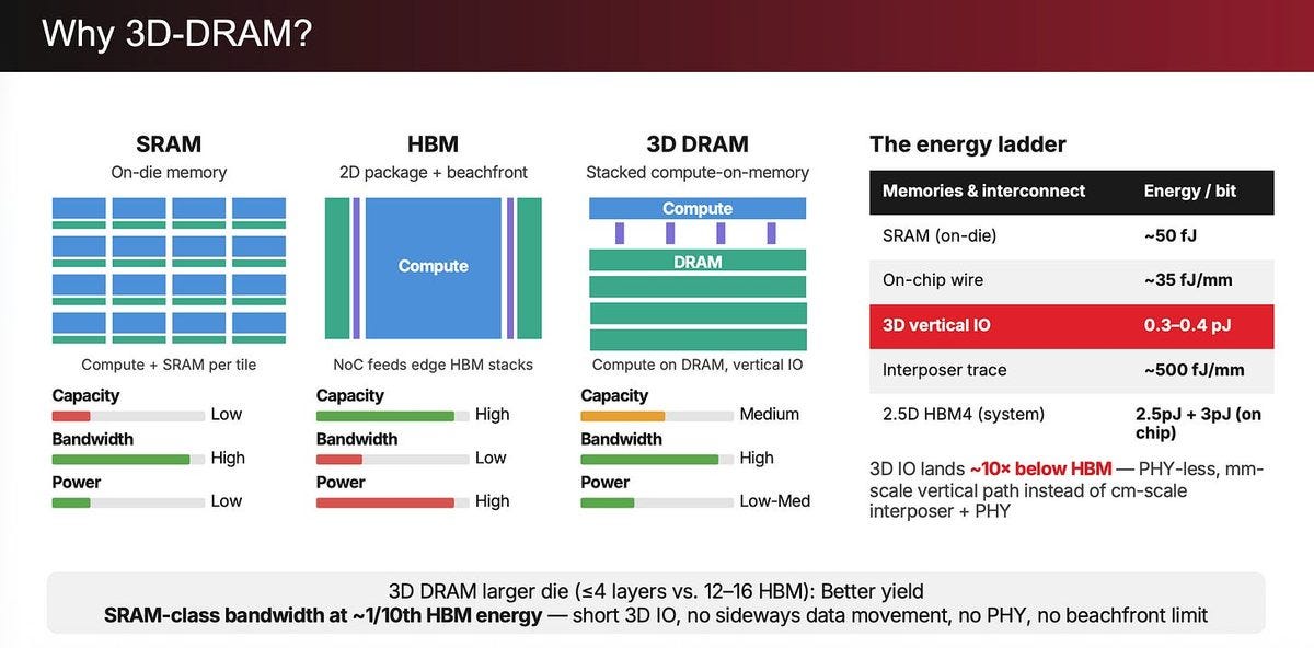
This presentation made the most radical memory idea of the conference sound obvious. SRAM (the fast memory that lives on the compute chip itself) is very fast but too big and expensive: a 6T SRAM cell is 10x larger than a DRAM cell, leaks tens of watts at GB scale, costs about 100x DRAM per bit, and tops out around 4GB per card pair. HBM has great capacity but is no longer high bandwidth enough, with a practical limit around 20 TB/s per package even on HBM4, because the number of stacks you can place is limited by the GPU die’s beachfront, the physical edge length available for connections.
The d-Matrix solution is stacking compute directly on memory, which they call 3D DRAM. It has high bandwidth because there is no beachfront limitation (the connections go down through the whole face of the die rather than around its edges), and high capacity because it is still DRAM underneath. Their Raptor chiplet puts the logic die on top and the DRAM below it, and the numbers are wild: SRAM-class bandwidth at roughly 1/10th the I/O energy of HBM, around 100 TB/s per chip, with no PHY and no sideways data movement.
Provide a caption (optional)
Most of inference wall-clock time is spent on decode, so this is aimed straight at the expensive phase. The pitch is 3D DRAM equals speedy inference that does not bankrupt you: their comparison table shows 32.6 GB/s of bandwidth per mm2 of silicon versus 1.4-1.7 for HBM4 systems, at 2.96 mW per GB/s versus 40 for HBM.
The appeal is simplicity: while the rest of the industry pursues more complex escapes, d-Matrix stacks the logic directly on the DRAM: 4 layers maximum (better yield than 12-16 layer HBM stacks), and no hybrid bonding required.
High Bandwidth Flash
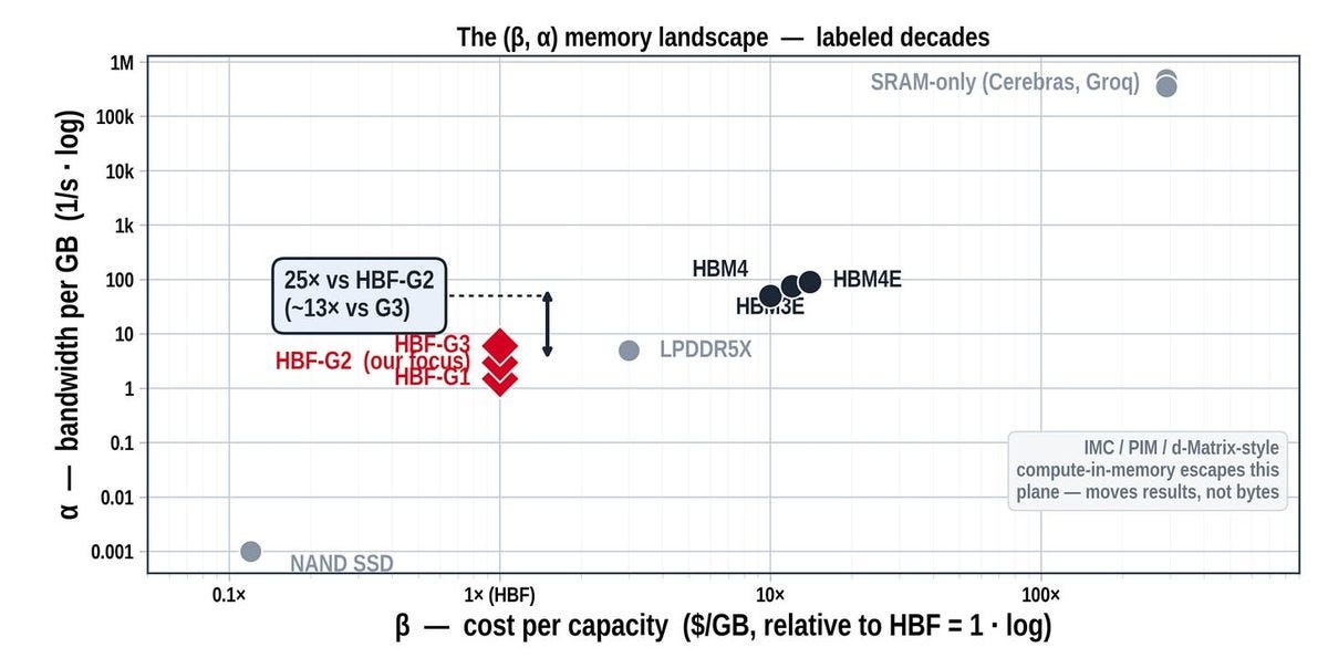
The HBF talk was the systems reality check of the memory day. HBF stacks NAND the way HBM stacks DRAM, giving 8-16x the capacity of HBM at the same cost, and the presenters (OXMIQ and PRAXMATI, working from the SanDisk-aligned spec) spent the whole session on when that trade actually wins. What people actually care about is $/token rather than $/GB, so you have to consider the bandwidth and latency tradeoff, which is roughly 25x worse than HBM.
Provide a caption (optional)
Memory bandwidth binds when you have high batch size (many user requests served at once, which is where throughput comes from) and high interactivity (speedy inference). The 2 trade off against each other, and bandwidth is what constrains you whenever you push the frontier of that tradeoff.
When you push that frontier, HBF has tons of unused capacity and its bandwidth ceiling caps you. Their own rack math shows it honestly: an all-HBF GPU carries 4,096GB against 288GB for HBM-only, but effective bandwidth decays from 19 TB/s toward 4 TB/s as batch size rises. So HBF is useful in low batch, low bandwidth-demand scenarios, where you can serve the same tokens with fewer GPUs and actually fill the capacity. Think a small personal, local, or private enterprise deployment rather than a big rack.
The other interesting use case is expert parallelism, where a mixture-of-experts (MoE) model’s experts (the big feed-forward blocks that hold most of its weights, of which each token only uses a few) get spread across separate GPUs. HBF thrives here because more of the experts fit in the same place, so you cut down the cross-GPU communication that expert parallelism normally requires.
I was bullish on HBF going in and came out slightly less bullish and with more realism. SanDisk’s investor day presented the maximal version of the case, and the conference version restored the bandwidth trade-off. What keeps me constructive is the maturity gap: consider how much R&D has been poured into the HBM ecosystem versus HBF, which is at generation 1. A few niche use cases existing today, before the software and the system design have matured, reads as bullish for where the trade-off lands in 3 years. And adoption would move NAND demand disproportionately, because the trade ratio is enormous. HBF needs SLC instead of TLC (3x the die per bit) and then stacks like HBM, which gets you to something like a 9x consumption multiple on the NAND it displaces.
Samsung LPDDR5X-PIM
Memory-themed presentations continued on day 3 with Samsung’s second processing-in-memory talk, and the persistence is rational: Samsung is the only memory maker that can do this end to end and capture the benefit. The talk opened with the chart of the conference: memory (mostly HBM) has grown from 52% of AI chip component cost in Q1 2024 to 63% by Q4 2025. Present that chart to a room of system designers and every one of them hears the same thing: the biggest cost line is the one to engineer away.
Provide a caption (optional)
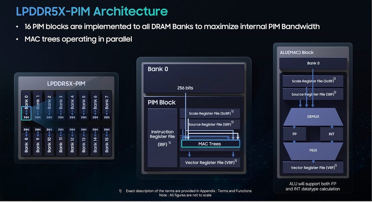
PIM here means a small logic block next to each DRAM memory bank, this time inside LPDDR5X rather than HBM. The banks feed the logic blocks in parallel, which supports 8x the internal bandwidth of the LPDDR5X external interface, and with processing next to the banks you only send back the data that actually needs to go to the main processor.
It can be used for both server and edge, with the GEMV-heavy parts of small-model inference running in the memory itself. I do not know what a module like this costs from Samsung, but the potential is visible, especially for the class of low-batch workloads where a full GPU is overkill and the memory bus is the whole bottleneck.
XCENA MX1
The MX1, jointly presented with Samsung, extends the same near-memory logic one tier further out, onto the CXL expansion bus. CXL is memory pooling that improves utilization and expands capacity arbitrarily. The MX1 is a Type 3 CXL device carrying up to 2TB of DDR5, with SSDs behind it that software sees as actual memory while the DRAM is the cache. They call it infinite memory, and it is bullish for NAND, since it invites NAND into DRAM’s memory tier by solving part of the latency problem.
The near-memory compute part is the more interesting half. MX1 carries 3,072 small RISC-V cores, which makes it a CPU with nowhere near the TFLOPS of a GPU (about 3 TFLOPS total) that is nonetheless programmed like a GPU, with kernels, jobs, and a map-style runtime.
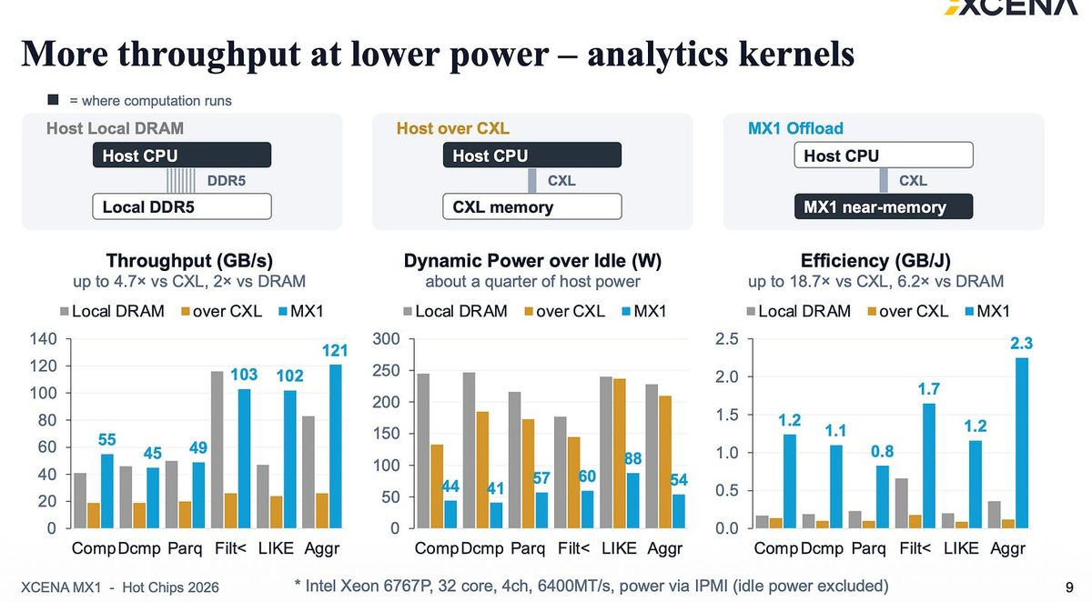
The point of those cores is data reduction where the data lives. Run analytics on the host from local DRAM and you get baseline throughput. Move the data out to plain CXL memory and throughput collapses, because every byte crosses the link. Run the compute on the MX1 itself instead, and throughput comes back above the local-DRAM baseline at about a quarter of the host power, since only answers cross the link instead of raw data.
Provide a caption (optional)
The LLM demo is the one to remember: KV cache attention computed on a pool of MX1 devices instead of shipping the cache to the GPU, for 3.35x decode throughput at 100K context. The hardware is small and the numbers are lab-scale, but the architecture is right.
Memory Takeaways
The memory day produced 5 approaches: logic on the HBM base die, compute stacked on DRAM, NAND stacked like HBM, logic inside LPDDR banks, and RISC-V cores on the CXL expander. That is 5 different bets, from 5 different corners of the industry, on one thesis: moving data costs more than computing on it, so the compute must move to the data. Nobody coordinated this. When every player in an industry independently converges on the same architectural direction, the direction is settled, and the spend follows.
Near term, everything presented here is 2-4 years from volume, so none of it relieves the shortage that is currently repricing DRAM and NAND. The 3x (HBM) and 9x (HBF) trade ratios keep tightening supply of commodity bits in the meantime. Long term, this queue of technologies exists to compress the memory bill.
CPUs
Day 2 was all about processing units, both the central kind and the graphics kind. The CPU half of the day was really a single debate: what should the host processor next to the GPUs actually be? Agentic workloads changed the question, because an agent chain is a serial sequence of model calls, tool calls, and orchestration steps, and the CPU sits on the critical path of every link. 6 companies gave 6 different answers, and the spread between them is the widest I have seen in 10 years of server CPUs.
IBM Z and LinuxONE
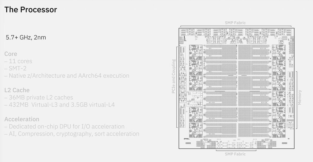
IBM is entering the Arm ecosystem. The next mainframe processor is dual ISA: it executes both z/Architecture and Arm v9.3 natively, in hardware, on the same core. The core itself is enormous by Arm standards, 5.7+ GHz on a 2nm process, with the mainframe’s usual giant caches behind it, so it delivers very high single-core performance for an Arm CPU. This is a next-generation part, so none of it ships soon.
Provide a caption (optional)
The mainframe’s structural problem for decades has been its shrinking software ecosystem, and running Arm Linux natively (with the Z accelerators for crypto and AI exposed to the Arm side) attacks that problem directly. They also showed the next Spyre AI card, with 96GB of HBM3E at 4 TB/s for enterprise inference, so even the mainframe now carries an HBM line item.
Intel Wildcat Lake
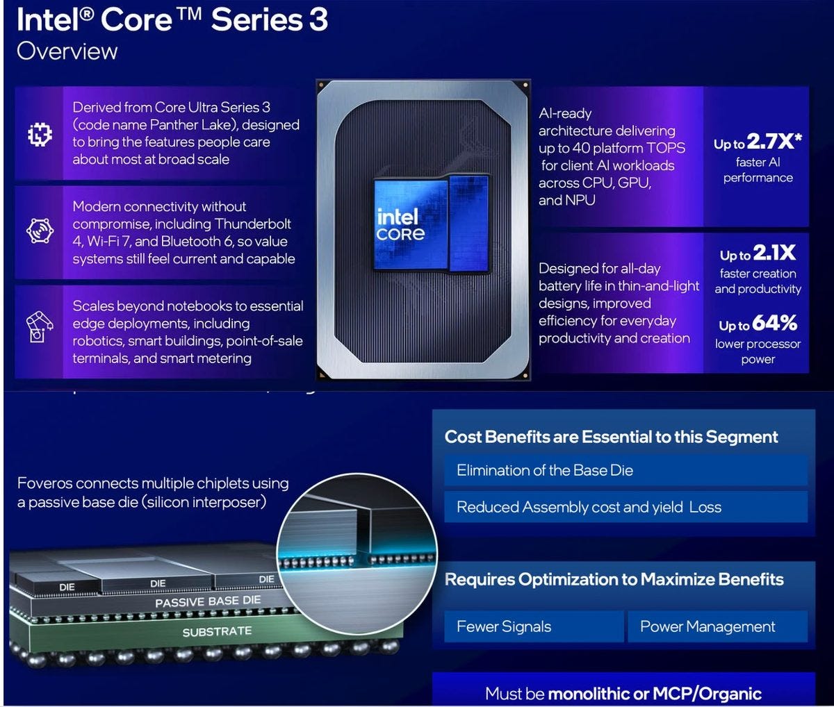
Wildcat Lake is a client CPU for desktops and laptops rather than datacenters. It already launched earlier this year as Core Series 3, and the talk was about how it was built, which turned out to be more interesting than the chip. Wildcat Lake is the value-tier derivative of Panther Lake, fabbed on 18A, and the whole program was a cost-reduction exercise: they swapped the Foveros silicon interposer (a slice of silicon under the chiplets, the separate small dies that get packaged together into 1 processor, routing the signals between them) for a cheap organic package, shrank the GPU, NPU, and memory bus to mainstream sizes, and cut die area 38% on compute and 15% on I/O.
Provide a caption (optional)
The one real innovation is using UCIe (the open chiplet-to-chiplet interconnect standard) on that cheap organic package, which per Intel nobody had shipped in a mainstream client CPU before. The interface came out 70% larger than the Foveros version and they took the trade anyway, because eliminating the interposer pays for it.
NVIDIA Vera
Vera was the first directly AI-relevant presentation of the day. The core pitch for Vera is maximal single-thread performance. This is the bet that agentic workloads need minimal latency and do not care much about throughput, the way desktop multitasking does. The model reasons, calls a tool, waits for the CPU to execute it, and reasons again, so every millisecond of CPU latency stacks into the user’s total response time.
Speeding up common agent operations such as headless browser use was a benchmark slide, with a claimed 4.5x on browser instances. The resulting design choice is a big core: 88 custom Olympus cores at the socket level, built out of 6 dies with the massive core die in the center.
Provide a caption (optional)
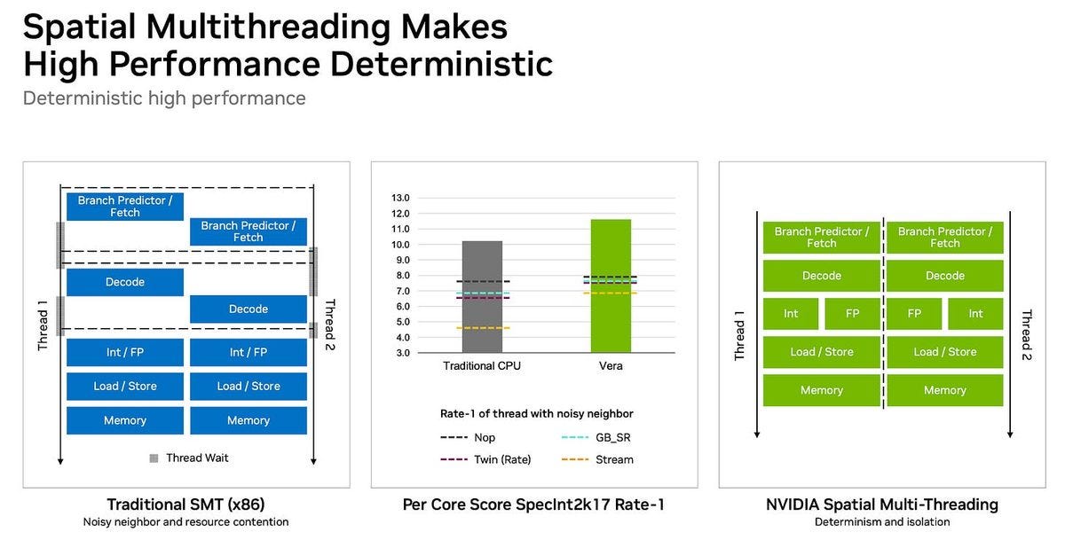
They have a type of multi-threading that is not traditional SMT (simultaneous multi-threading), called spatial multi-threading. Spatial means the 2 threads on a core get physically separate resources instead of sharing them, so no thread can stall its neighbor. That makes performance deterministic. In their SPECint chart, a traditional x86 core’s throughput swings wildly with a noisy neighbor thread, while Vera’s stays in a tight band. For serial agent chains, where the slowest step gates everything, predictable beats fast-on-average.
Traditional SMT is statistically more efficient, since a stalled thread donates its whole core to its neighbor. Spatial partitioning trades that aggregate throughput for isolation, and the duplicated front-ends cost die area on top. Vera lands at 88 cores where EPYC and Graviton5 field 192. The LPDDR5X memory gives 5x the bandwidth per watt of DDR5, but it is soldered, which means capacity ceilings versus socketed DIMMs and worse serviceability. And the deck never shows SPECrate throughput per socket, which is the number cloud economics run on. I think Vera only makes sense as a co-designed orchestration processor welded into NVIDIA’s rack, and on those terms the design is coherent.
FUJITSU-MONAKA
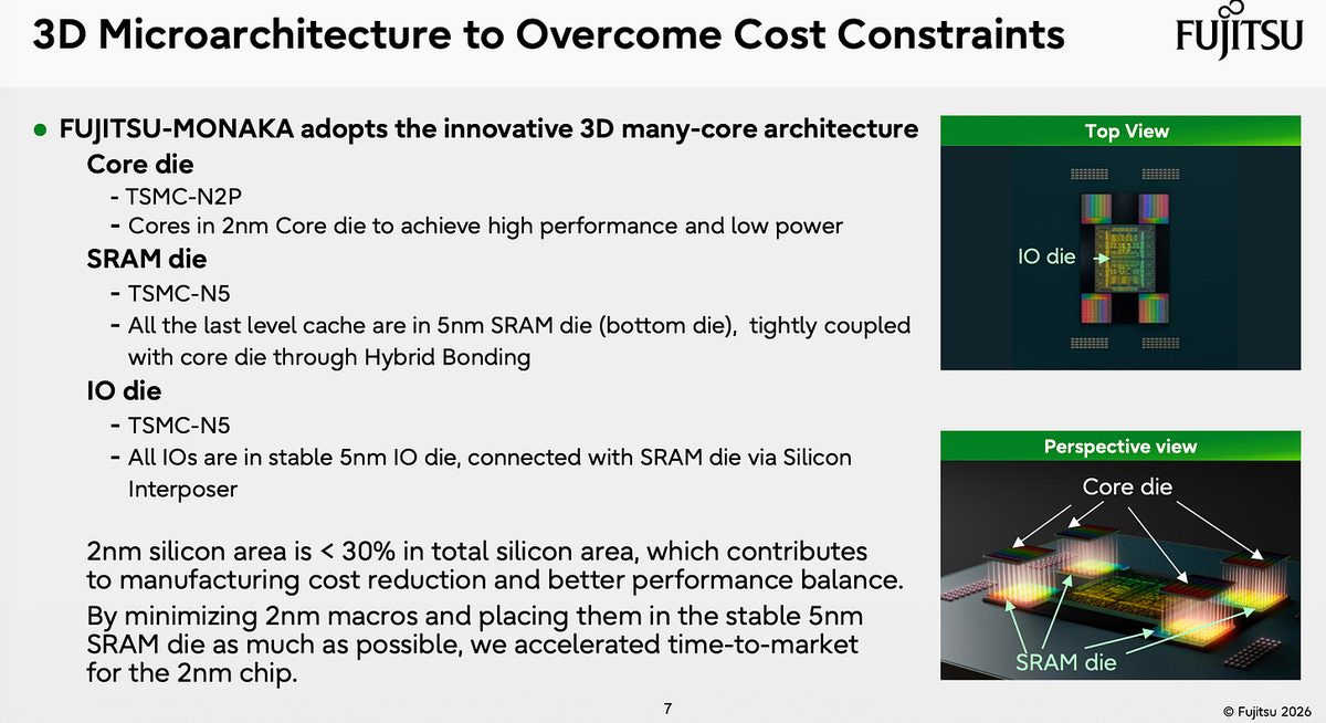
MONAKA is Fujitsu’s 144-core Arm server chip (288 cores per 2-socket node) aimed at green datacenter compute, sampling now and shipping in 2027, and the interesting part is in how it is built. Their core pitch is not using 2nm for everything: the cores go on a TSMC N2P die, while all the SRAM last-level cache and all the I/O go on 5nm dies underneath, connected by hybrid bonding, with the hot core die on top where the cooler can reach it.
Provide a caption (optional)
This optimizes for cost and power, and it works: SRAM and analog circuits barely shrink below 5nm anymore, so paying 2nm wafer prices for them buys nothing. Under 30% of MONAKA’s total silicon is leading edge. They also park the voltage regulators on the 5nm SRAM die directly beneath the hottest compute blocks, which enables per-core voltage control and their ultra-low-voltage trick (running 30% below nominal voltage for half the power). Putting core dies on opposite sides of the chip does raise a core-to-core latency question that the talk did not really answer.
Arm AGI
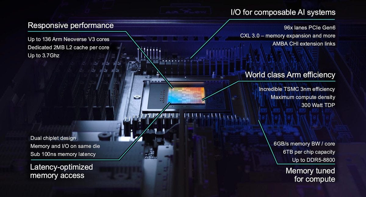
Arm is making a chip for the first time instead of only licensing IP. Before, you could use their Neoverse cores for your own designs, and now they are using their own IP to make their own finished CPU, with Meta as the lead customer. The chip itself runs up to 136 Neoverse V3 cores across 2 chiplets connected by UCIe, on TSMC N3P, with 12 channels of DDR5-8800 for 845 GB/s and up to 6TB of capacity, 96 lanes of PCIe Gen6, at 300W.
Provide a caption (optional)
The design takes no strong view on the market the way Intel and NVIDIA do. Stock cores, standard DIMMs, moderate power, no exotic anything. The 300W power envelope is the one differentiator, at 2.2W per core against 400-500W sockets from the x86 camp, and in a power-constrained datacenter that is a legitimate pitch. The more important point to me is that they are making a chip in the first place, and that every Arm licensee from Ampere to the hyperscaler CPU teams now competes with its own IP supplier.
Intel Diamond Rapids
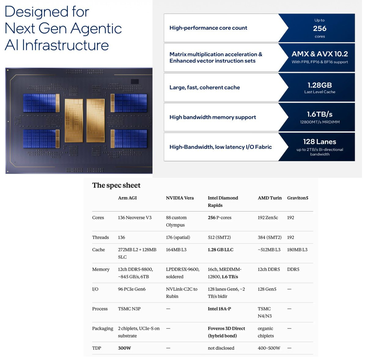
Intel’s next Xeon is a spec sheet with a fan-out fabric architecture, and the specs are extreme. The construction is a set of compute building blocks surrounding a central I/O and memory fabric hub, with core chiplets hybrid-bonded on top of base tiles that hold the cache.
It is very scalable because you add more compute building blocks to one chip, and the result is 1.28GB of last-level cache, 256 cores, and 512 threads, fed by 16 channels of DDR5 that reach 1.6 TB/s with MRDIMMs, plus 128 lanes of PCIe Gen6.
That is 3x the cores of Vera (88) and more than EPYC and Graviton5 (192 each). On cache it is 5MB of LLC per core, versus Arm AGI at 2.9MB, Vera at 1.9MB, and Graviton5 at 0.94MB. This chip is the polar opposite of Vera, and Intel is taking its own strong view on the market. They never claim a different workload; it is for agentic too. They simply emphasize different specs: where NVIDIA argues agents need per-core latency, Intel argues agents need a giant cache to hold their working state and maximum aggregate throughput to serve many of them at once. The deck never shows TDP, frequency, or any competitive benchmark.
Provide a caption (optional)
And then every part of the chip is Intel-made, including the 18A-P process and the Foveros Direct 3D packaging. No TSMC anywhere in the bill of materials.
CPU Takeaways
No two vendors agree on what the host CPU even is. NVIDIA says it is a latency device with 88 deterministic cores, and Intel says the opposite, a throughput device with 256 cores and 1.28GB of cache. Arm calls it a commodity at 300W, for Fujitsu it is a packaging problem, and for IBM it is an ecosystem problem. For 10 years server CPUs converged on 1 shape. The agentic workload broke the consensus, because nobody actually knows yet whether agents bottleneck on single-thread latency, cache capacity, core count, or power.
GPUs
The GPU talks stopped being about GPUs somewhere around Blackwell, and this year made it official: NVIDIA and AMD both presented racks, and Intel presented a card precisely because it cannot yet present a rack. The unit of account in every chart was the 72-GPU scale-up domain (the set of GPUs wired together tightly enough to act as 1 big accelerator), the axis on every chart was the throughput-interactivity curve (cheap tokens at one end, fast tokens at the other), and the differences between vendors live in what each one chose to put on that curve.
NVIDIA Rubin
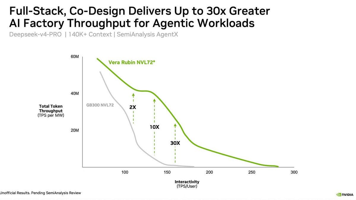
The performance boost of Rubin over Blackwell is bigger on the high-interactivity (fast tokens) side than the high-throughput one: 2x throughput per MW at low interactivity and 30x at high interactivity, on their DeepSeek agentic benchmark. We will see much faster tokens within a year.
Provide a caption (optional)
The 30x number is the whole strategy. The gain grows as you move right on the curve because the platform now attacks decode speed specifically, and part of that attack sits outside the GPU. Groq LPX (NVIDIA bought Groq, and the LPU got its own talk) disaggregates the decode and speeds it up. When the constraint is memory bandwidth and the goal is speed, SRAM is the answer.
“No one uses a single chip” was the framing, and I agree with it. The platform now spans 7 chips across 5 racks, with Rubin NVL72 as the foundation, Groq LPX extending interactivity, Vera handling tool calls, BlueField-4 doing context storage, and Spectrum-X scaling out.
On the silicon itself, the headline feature is adaptive sparsity. Quantization (how many bits each model weight gets, FP16 versus FP8 versus FP4) is specific to the hardware and has to be supported by it. They went FP16 to FP8 to FP4 across generations, but FP2 is a step too far, because model quality collapses. So they went sideways instead: take the model, drop the values that are near zero to make it half as big, and replace them with metadata that tells the hardware where the holes are. NVFP4 is a less brutal version of FP4, sitting between FP8 and FP4 in quality, and the sparsity rides on top of it. They also do sparse attention, where you only attend over the tokens that matter instead of every token in the context, natively supported on Rubin. The pattern across both features is the same: inference optimization tricks that used to live in software, baked into the hardware generation.
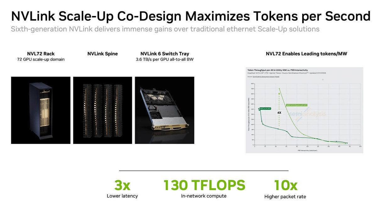
NVLink is an important moat for NVIDIA, and the scale-up slide is where the economics live. Large scale-up domains let racks win on the high-throughput (cheap token) side of the curve via expert parallelism. A bigger domain means a MoE model’s experts spread across more GPUs, so each GPU reads fewer weight bytes per token, and the pooled memory holds bigger batches. It is the exact opposite end of the curve from the Groq LPX, and the platform now owns both ends.
Provide a caption (optional)
Some features of the rack: no optics (yet), 800VDC power with a sidecar, minimized cables, chiller-free 45C liquid cooling, and power smoothing with energy storage that shaves 13% off peak draw.
AMD Instinct MI400 and Helios
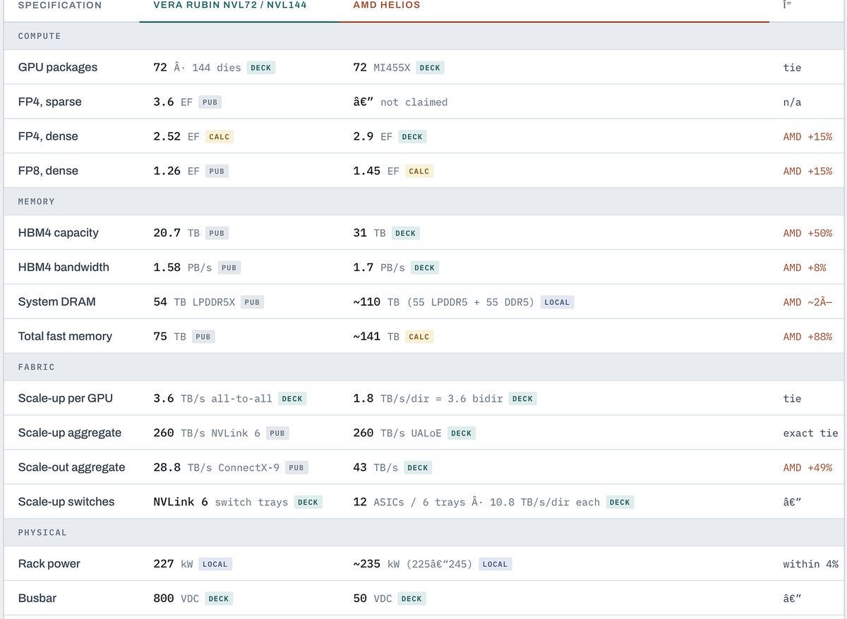
AMD built its own 72-GPU rack, and on published specs it is more than competitive. Helios is built from MI455X accelerators, and it beats or ties the NVIDIA VR200 NVL72 on nearly all the published specs. FP4 FLOPS and scale-up bandwidth are tied, and AMD wins everything else.
Provide a caption (optional)
AMD wins especially on memory capacity (31TB of HBM4 per rack versus 21TB) and scale-out bandwidth (43 TB/s versus 28.8). The racks land at almost the same power, so technically you get denser per-MW performance. This is the AMD catch-up the market has been anticipating. MI455X stacks 432GB of HBM4 at 23.3 TB/s from 12 stacks, built as 12 chiplets across N2 compute dies and N3P for everything else, on CoWoS-L (TSMC’s advanced packaging, itself one of the constrained inputs).
What NVIDIA has that AMD still does not is NVLink, a protocol co-designed with all its GPUs and deliberately not an open standard. When you do all-to-all collectives (every GPU exchanging data with every other GPU at once), the speed of the system is the speed of the slowest participant, so you need to cut the tail. AMD’s UALink-over-Ethernet answer hits the same 260 TB/s aggregate bandwidth on merchant Broadcom switches. The hard part is tail latency under load, and neither vendor publishes that number. And CUDA barely came up, because NVIDIA no longer needs to argue the software point.
NVIDIA focused purely on system-level performance while AMD’s slides are a giant spec sheet, and the difference is the competitive story. NVIDIA, as the incumbent, has all the models and software co-designed around it, so it can lean on maturity and sell system-level results. The only way AMD catches up is winning on pure specs, and to their credit, the deck also shows measured numbers (20 TB/s decode bandwidth, measured scale-up, measured scale-out) rather than only peaks.
The system talk showed the pod architecture: each tray is 4 GPUs and 1 EPYC Venice connected up to 12 scale-up switch ASICs across 6 trays, with graceful degradation if a link, a switch, or a whole switch tray dies.
They said the generation after this one goes optical, same timing as Rubin Ultra. AMD is not adopting 800VDC just yet, and the rack is a double-wide, whereas NVIDIA’s is a single-wide.
Intel Crescent Island
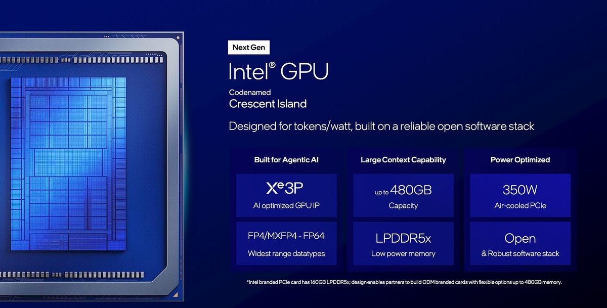
This is Intel’s new attempt at a datacenter GPU, and the design refuses every convention of the category: no HBM, air-cooled, PCIe scale-up. It carries up to 480GB of LPDDR5X on a 350W card (Intel’s own card ships with 160GB, partners can build up to 480GB), built on the Xe3P graphics IP with MX-format datatypes.
Provide a caption (optional)
The obvious question is who would use this. It looks useful for cost-sensitive, latency-insensitive work, but for that you want to batch aggressively, and to batch aggressively you want a big scale-up domain, which PCIe cannot give you. Maybe local and small-enterprise private workloads. The answer that makes the design cohere is prefill. Use it for prefill only, and you barely need memory bandwidth (prefill, the prompt-reading phase, is compute bound), while the 480GB of cheap DRAM holds enormous contexts, double the per-GPU HBM of the big rack parts. Pair it with an SRAM-based decode part and you have a disaggregated inference pair assembled from parts that dodge the shortages: no HBM allocation, no CoWoS, no liquid cooling, and no fight for TSMC capacity.
GPU Takeaways
The rack has long replaced the chip as the product, and the throughput-interactivity curve has long replaced per-chip specs as the scoreboard. Each vendor chose where on the curve to live: NVIDIA bundles the whole curve. AMD attacks the spec-per-megawatt middle, and Intel is off in the prefill corner that needs no exotic components. Component demand follows the same logic, since a rack is a fixed budget of megawatts and dollars being allocated among HBM, fabric, cooling, and power, and every vendor just showed you a different allocation.
The number from these talks I keep coming back to is Rubin’s 2x-versus-30x split, because it says the next year of platform improvement lands disproportionately on token speed rather than token cost. Faster tokens change product experiences, and better experiences drive usage, which is the demand feedback loop. Cheaper tokens change unit economics, which caps how much hardware each token can carry. Both are happening, but the vendors are engineering hardest for the first one.
Networking
Networking got 3 dedicated talks, and together they show the AI network is no longer one thing. The new vocabulary says it: scale-up inside the rack, scale-out between racks, scale-across between datacenters, and now scale-in between the GPUs and the services around them. Each layer is becoming its own product category with its own physics, and the fight in every layer is the same fight, proprietary co-design against merchant Ethernet.
Broadcom Thor Ultra
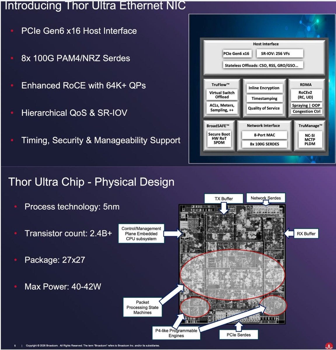
Broadcom’s NIC talk is the merchant side’s opening argument, and I got more out of it than I expected. Network interface cards (NICs) let GPUs talk directly to the scale-out network without going through a CPU, using remote direct memory access (RDMA) to read and write GPU HBM straight from the wire. This is also where the transceiver plugs in, which is why I track NIC count per GPU as an optics number.
Provide a caption (optional)
Thor Ultra is an 800G part on PCIe Gen6, 5nm, running 40-42W. The deck is structured as a confession list of what old Ethernet RDMA got wrong, each item now fixed per the Ultra Ethernet Consortium (UEC) playbook: no multipathing becomes packet spraying across up to 8 network planes, inefficient go-back-N retransmission becomes selective retransmission, and hard-to-tune congestion control becomes a programmable, receiver-credit-based scheme. Out-of-order packet placement is the clever bit, since sprayed packets arrive scrambled and the NIC writes them directly into their final GPU memory location instead of buffering to reorder. Their benchmarks on collectives (the all-GPU communication operations in training) land above 96% of line rate on 2 nodes, which is the number I would lead with if I were them.
NVIDIA BlueField-4
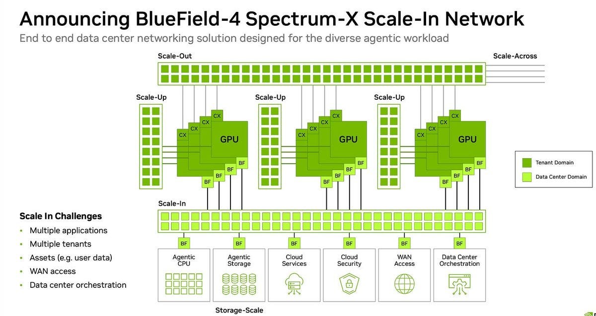
What does a DPU actually do? Data processing unit is not a very descriptive name; datacenter processing unit would be closer. It is a CPU that runs the infrastructure software (networking, storage, security) away from the main CPU so the main CPU can focus on the OS and applications. The deeper reason it exists is trust: the DPU is a server in front of the server, a separate processor with a separate OS, so the cloud operator’s control plane and the tenant’s code never share silicon.
Provide a caption (optional)
NVIDIA’s framing adds scale-in to the networking taxonomy: scale-up, scale-out, and scale-across connect GPUs to each other at varying distances, while scale-in connects GPUs to datacenter resources such as storage and security services. Agents made this a real traffic class, since an agent constantly hits databases, tool sandboxes, and context storage in between model calls.
BlueField-4 itself is a Grace CPU and a ConnectX-9 NIC on one package. The difference between an AI DPU and a traditional cloud DPU is the bandwidth: 7.2 Tb/s per compute tray, versus 200 Gb/s for the cloud DPUs of 2021. The talk also productized a 5-tier KV cache hierarchy (GPU HBM for active context, system memory for spillover, local NVMe for warm reuse, network storage for cold context), orchestrated by the DPU, with a claimed 5x power efficiency on context storage.
NVIDIA Spectrum-X
Spectrum-X is NVIDIA’s Ethernet scale-out, custom designed for higher bandwidth and lower jitter (variance in latency), and per the talk by now well ahead of Infiniband in adoption. Multi-tenancy is when one fabric carries multiple jobs at once, and Spectrum-X was designed for it specifically, with 1.9x better training performance in a multi-job environment against off-the-shelf Ethernet. The single-job gap is only 1.2x, and that spread is the whole product: the value shows up when neighbors get noisy, which in a real cloud is always.
NVIDIA’s optics section answered a question I have been asked a lot. We know why you need CPO (co-packaged optics, moving the optical engines from pluggable modules onto the switch package itself) for scale-up, but why for scale-out, which is already optical? The answer is power. Co-packaging eliminates the DSP (the signal-processing chip that exists to clean up the signal after the long copper trace from switch ASIC to faceplate). NVIDIA’s photonics numbers are 5x lower power, 4x fewer lasers, and 10x better reliability, on TSMC’s COUPE process, in production. They also sized optics at about 10% of an AI factory’s compute power, which is the sharpest TAM framing I have seen anyone hand the optical industry.
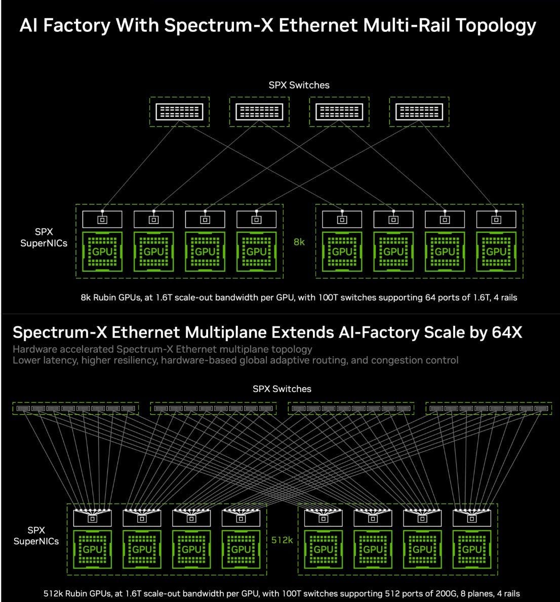
The main event is the multiplane topology. Traditional scale-out gives each GPU 1 fat port: a 102.4 Tb/s switch configured as 64 ports of 1.6T serves 64 GPUs per switch. The trick is configuring the same switch as 512 ports of 200G instead, and giving each GPU 8 thin ports into 8 independent network planes. Each GPU keeps the same total bandwidth, and the fabric now reaches 512K GPUs, 64x more, since 2-tier network scale goes with the square of switch radix (the port count). Any single link failure now costs a GPU 1/8th of its bandwidth instead of all of it.
Provide a caption (optional)
So this does a few things. First, the network becomes WAY more reliable, with 90% bandwidth retained through failures that take off-the-shelf Ethernet to 0, and 400x faster failure detection. Second, you need 1.7x fewer switches, which is bad for optics counts per GPU even as it enables the giga-scale clusters that grow optics in absolute terms.
Networking Takeaways
The fabric is following the same script as the compute: disaggregate the general thing into specialized layers, then fight over each layer separately. NVIDIA is ahead on co-designed behavior under load, with the merchant camp standardizing each generation’s tricks about 18 months behind.
The component read is that networking intensity per GPU keeps rising across every layer (a NIC per GPU becoming several, a DPU per tray, 8 planes per GPU), while 2 of these innovations (multiplane switch reduction, CPO laser reduction) cut content per port even as cluster scale explodes port count. Optics remains a volume story with a mix headwind, and the switch and NIC silicon remains a straight beneficiary regardless of which side wins the protocol argument.
ASICs
The last theme is the insurgents: 2 startups, a hyperscaler with a decade of silicon behind it, and a frontier lab that had never built a chip. All 4 talks share a diagnosis: decode is memory bandwidth bound, and general-purpose GPUs waste most of their bandwidth on it. All 4 share a prescription: SRAM close to compute, plus a topology tuned for low latency. The disagreements are about how far to push it.
Cerebras CS-4
Cerebras announced CS-4, and the announcement drew little attention. I think that is a mistake.
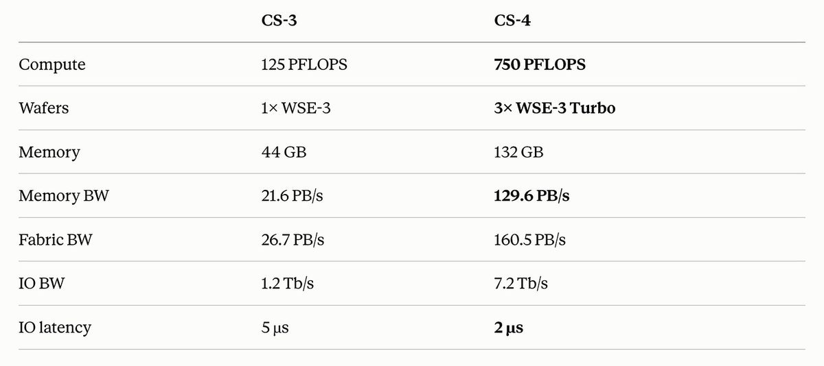
CS-4 moves from 1 wafer to 3 WSE-3 Turbo wafers per system: 750 PFLOPS (6x the CS-3), 132GB of on-wafer SRAM, and 129.6 PB/s of memory bandwidth, with new direct wafer-to-wafer links at 2 microseconds of latency.
Provide a caption (optional)
The architecture is the purest possible bet on the bandwidth thesis: keep the entire model in SRAM spread across the wafer, and the bandwidth number becomes 6,000x a Rubin GPU’s HBM. The cost is capacity, 132GB against 21TB in an NVL72 rack, so big models pipeline across wafers with only activations (the small intermediate results flowing between model layers) crossing between them, at less than 0.2ms per hop on a 10T-parameter model. That trade is why Cerebras owns the far right of the throughput-interactivity curve.
They also announced CS-6, which puts hybrid-bonded DRAM on the SRAM wafer. Enormous memory bandwidth with almost no memory capacity is the entire Cerebras limitation, and CS-6 is an attempt to remove it. If they solve the thermal issues associated with bonding DRAM to the wafer, the addressable market changes completely.
SambaNova SN50
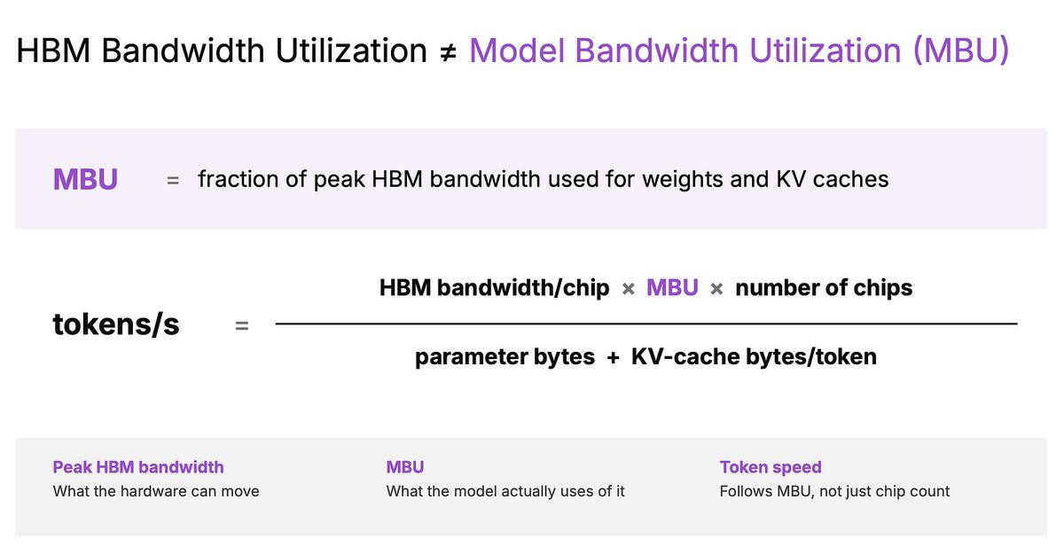
SambaNova’s argument is that decode is the bottleneck for inference, and HBM bandwidth is the bottleneck for decode. Most of the HBM bandwidth on a GPU is spent moving data that is neither weights nor KV cache. They built a metric around it, model bandwidth utilization (MBU), the fraction of peak memory bandwidth doing useful work, and their measurements put GPUs at 5-25% while the SN50 holds 44-51%.
Provide a caption (optional)
So they built SN50 as a decode specialist: 432MB of on-chip SRAM, 64GB of HBM per chip, and the software and chip design tricks that raise MBU. The 2 big ones: compiling the entire model into 1 persistent kernel (no kernel launches, no synchronization gaps, intermediates never round-trip through HBM) and spatial dataflow (lay the operator graph out physically across the chip and stream data through it, rather than time-slicing 1 big engine). The scaling claim is that MBU stays flat as chip count grows, 200 to 500 tokens per second per user from 64 to 256 chips, where GPU utilization collapses with scale.
Google TPU v8
Google’s change for TPU v8 is making 1 chip for training and 1 chip for inference, TPU 8t and TPU 8i, after a decade of alternating between the 2 on a single line.
The inference chip carries more HBM bandwidth per unit of compute, because decode is bandwidth bound. The 8i also carries a lot of SRAM (384MB, 2.4x the prior generation), plus 288GB of HBM3E in 12-high stacks. Their SRAM-versus-HBM table gives the whole custom-silicon story its numbers: 15-20x the bandwidth, 100x lower latency, 10-20x better energy per bit.
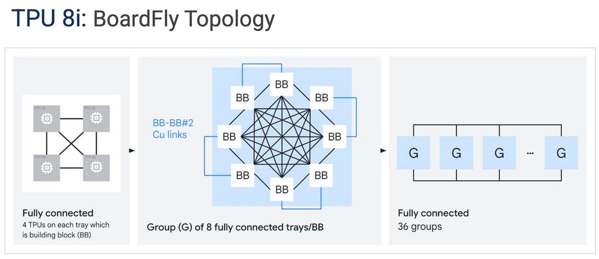
The networking topology is the other change. The 8i uses a new arrangement they call BoardFly, 1,152 chips per pod with a maximum of 7 hops between any 2, versus 16 hops in the old 3D torus. The point of fewer hops is lower latency, because MoE all-to-all traffic is bound by network latency. They also put collective operations into the interconnect die itself, cutting another 5x of latency.
Provide a caption (optional)
In training you need bisection bandwidth instead (the bandwidth across the middle of the network when you cut it in half), so the 3D torus remains, with lots of optical circuit switching (OCS). Training needs lots of FLOPS and lots of shared memory: the 8t superpod is 9,600 chips sharing 2PB of HBM at 121 exaflops, any slice size carved on demand through the OCS layer, as typical of Google.
OpenAI Jalapeño
OpenAI closed the conference with Jalapeño, the inference chip it had announced the morning of day 2.
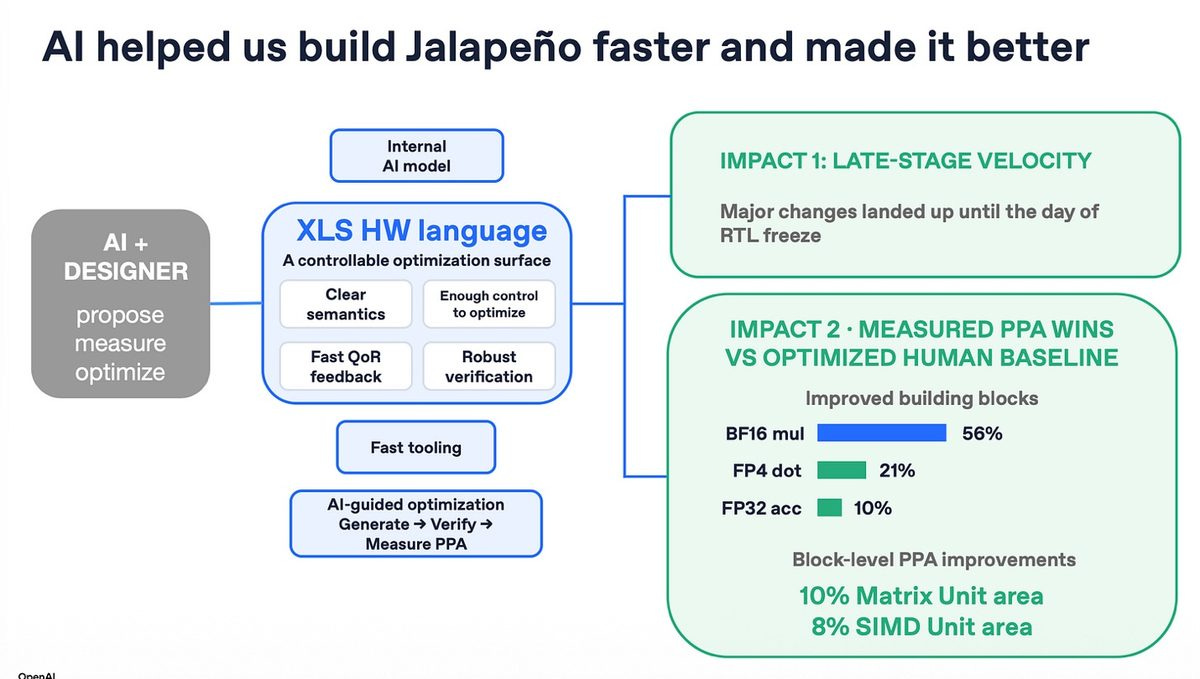
They taped out in 9 months with an extremely small team, and one of the first things they said was that their internal AI system helped them build the chip. There was barely any traditional chip design experience on the team. The chip itself: a compute die with an I/O chiplet and 6 HBM4 stacks, 216GB at 15.4 TB/s per chip, 700W, designed for OpenAI’s inference workloads. It was designed around speculative decode, which is using a cheap draft model to predict several tokens ahead and then checking them with the main model in 1 batched pass, turning 8 serial trunk passes into 1.
They built it for both prefill and decode and for both throughput and interactivity, trying to be the Pareto frontier everywhere, and the benchmarks are aggressive in the right way: power-normalized comparisons on the public SemiAnalysis InferenceX suite, on models never co-designed for the chip, with Jalapeño running plain single-token prediction against GPU baselines allowed speculative decoding. They claim the frontier anyway, 1.7x tokens per kW over GB300 on DeepSeek R1 with 3.6x lower latency, which is a remarkable result for first silicon. The improvement is much bigger on the high-interactivity side than high-throughput, same shape as everyone else this year.
A rack holds 128 Jalapeños, over 1 PB/s of aggregate memory bandwidth, in the same neighborhood as a VR200 NVL72, with Broadcom Tomahawk 6 for the network. The smartest thing they did, though, is the process rather than the chip.
Provide a caption (optional)
They kept the team tiny so it could move fast. More importantly, they built a new hardware description language, similar in spirit to Rust, designed so AI could write correct code out of the box, and ran an internal AI optimization system over the design from functionally-correct to beyond-expert performance. They went from RTL freeze to tapeout in 9 months and from first silicon to serving ChatGPT in 10 weeks, with generation 2 already approaching tapeout.
ASIC / Inference Startup Takeaways
The insurgents used to be a zoo of incompatible bets, and this year they converged: big SRAM, low-hop topologies, decode specialization, and a seat on the throughput-interactivity curve chosen in advance. Convergence means the architecture argument is settling and the fight is moving to manufacturing access, software maturity, and capital. That fight favors the players attached to hyperscaler balance sheets (TPU, Jalapeño, and the acquired Groq) over the independents selling into the same sockets.
Conference Takeaways
My top 4 conclusions for Hot Chips 2026.
Capitalism Is Coming for the Memory Markup
There is a staggering amount of innovation happening in the memory layer right now, and the reason is price. Memory makers are extracting something like 90% gross margins on HBM-class products, which is a 10x markup over cost, and this is classic economics: when a markup like that exists, the forces of capitalism combine to destroy it and relieve the shortage. That is easy to say in a business school macro way, and it is a different thing entirely to shrink down to the micro level and watch 1 building block of the process actually happen. This conference is that building block: Samsung putting logic in the base die, d-Matrix stacking compute on DRAM, SanDisk-aligned HBF stacking NAND like HBM, Samsung again with logic inside LPDDR banks, XCENA with compute on the CXL expander, Cerebras bonding DRAM onto wafers, and every accelerator vendor substituting SRAM for HBM wherever the workload allows. All the HBM despec talk you hear in the market is the same force wearing supply-chain clothes: buyers redesigning systems to need less of the expensive thing per token.
None of this lands in time to break the current cycle, since all of it is 2-4 years from volume, and several of the escapes (HBF, HBM4 base dies) actually consume more wafers per bit on the way. So the near-term shortage stands. The medium-term lesson is that the markup is rented, and the rent is being contested from 6 directions at once. The memory makers know it, which is why Samsung’s entire conference presence was about climbing the value stack before the commodity layer gets arbitraged.
Disaggregation Is Eating Inference
The second theme I could not stop seeing: inference is being taken apart into phases, and each phase is getting its own hardware. At the high level, prefill and decode split, since prefill is compute bound and decode is memory bandwidth bound, and running both on the same GPU wastes one resource or the other. Intel built Crescent Island explicitly for the prefill side. SambaNova, Groq, Cerebras, and d-Matrix built explicitly for the decode side. NVIDIA productized the split inside its own platform, with the LPX drafting tokens and Rubin verifying them, and BlueField tiering the KV cache underneath. One level lower, the same knife cuts again: attention offloads to near-memory devices (the XCENA demo), experts spread across cheap-capacity memory (the HBF case), and speculative decode splits the token loop itself (Jalapeño’s whole design center).
You see the throughput-interactivity curve in basically every deck, and that repetition is the tell. An immature industry built maximally general chips because nobody knew how the workload would evolve, and now that the workload is legible, everyone is pulling the general thing apart and squeezing each piece. The engineering trades are additive: the same hardware resources serve meaningfully more tokens after disaggregation, since each phase runs on silicon shaped for it.
If you assume chips and memory scale proportionally with token demand, disaggregation breaks it, since the industry is actively figuring out how to serve more tokens per unit of everything. Efficiency gains this large usually resolve through Jevons dynamics, cheaper and faster tokens creating more than proportional token demand, and that has been the right bet at every prior efficiency step. But the composition of demand shifts even when the total grows: decode-specialized silicon carries different memory (more SRAM, sometimes no HBM), prefill tiers carry cheap LPDDR instead of HBM, and KV cache migrates down the storage hierarchy toward NAND.
AI Is Coming for Chip Design Itself
OpenAI’s talk was, I think, the most important 30 minutes of the conference, mostly for reasons that have nothing to do with the Jalapeño chip. The talk showed a tiny team with barely any silicon veterans, a custom AI-friendly hardware language, an internal AI optimization loop, and RTL to tapeout in 9 months, landing a part they credibly claim beats the incumbent on power-normalized inference. Chip design has been defended by scarce talent compounding inside a few companies for 40 years. It also happens to be a nearly ideal domain for AI: fully digital, simulation rich, and verifiable at every step, so an AI can check its own work the way it cannot in most of engineering.
Over the long term I think this is pretty bearish for any fabless chip designer whose moat is design talent and iteration speed rather than ecosystem lock-in. This feels like how chip design should be done. In software, a giant corporation with 2,000 engineers is exactly who gets disrupted when a small, AI-native team with a proper harness can ship the same artifact in a fraction of the time, and semiconductor design might not be too different. The giants have the talent today, but talent can be poached, and harnesses can be copied. The moats that survive this are the ones AI does not compress: manufacturing access and allocation, installed software ecosystems, customer relationships, and fabs. That is roughly NVIDIA’s actual moat stack (CUDA, NVLink, supply relationships). A mid-tier ASIC vendor has almost none of it, and its entire value proposition (design execution as a service) is the thing that just got cheaper. EDA is the second-order question: the volume of design starts goes up, while value per seat gets contested by exactly the tools the labs are building for themselves.
Leading Edge Is for Logic Only
The fourth conclusion is one I had to assemble from 4 unrelated talks: the leading-edge wafer is becoming a scarce input reserved for the transistors that actually benefit, with everything else partitioned onto trailing nodes and rejoined through advanced packaging. Fujitsu put under 30% of MONAKA’s silicon on N2, with the SRAM and I/O on 5nm, because SRAM and analog stopped shrinking. AMD did the same to the MI455X, N2 for the compute dies and N3P for everything else. Samsung’s whole custom HBM pitch is moving the base die to whatever node earns its keep, and Intel built Wildcat Lake’s cost story on organic packaging and right-sized dies. Nobody presented this as a shared thesis, and it is one.
Thus, this could mean leading-edge wafer demand per chip grows much slower than transistor counts suggest, while packaging intensity (hybrid bonding, die-to-die interfaces, substrates) grows much faster. That is structurally bullish for the packaging and bonding toolchain and for trailing-node capacity utilization.